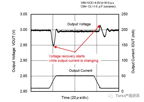
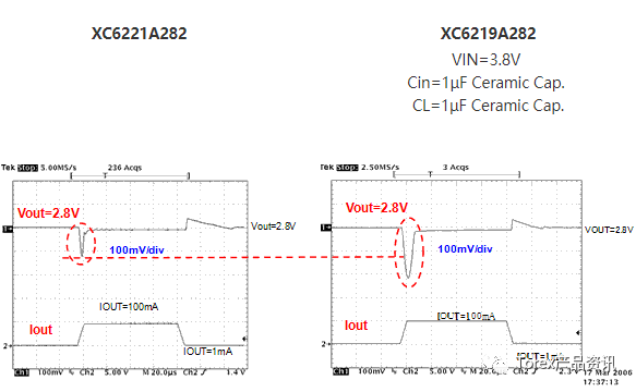
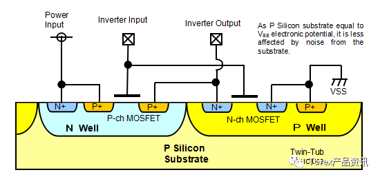
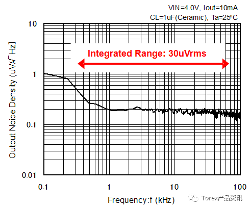
Transient response characteristics The transient response characteristic refers to the following characteristics when the input voltage or load current changes in a stepped manner. As the trigger mode is used in the digital signal processing of electronic instruments, the load current of the LSI or the memory IC changes more. Therefore, it is required to continuously improve the transient response characteristics of the regulator to follow its changes. Transient response characteristics include input transient response characteristics and load transient response characteristics, and the linear regulator's transient response characteristics are dependent on the circuit's current consumption. Here, the gate capacitances of the error amplifier and the output P-channel MOS transistor shown in the basic internal circuit block diagram (first FIG. 4) are looked at. The CMOS linear regulator is equipped with a larger output P-channel MOS transistor. The output impedance of the error amplifier and the gate capacitance of the MOS transistor required to drive the P-channel MOS transistor basically determine the response speed. The output impedance of this error amplifier is determined by the current consumption in the circuit. The greater the current consumption, the lower the impedance and the high speed response. A high-speed type product is inserted with a buffer for improving driving capability, and the buffer can also function as an amplifier, thereby forming a primary (error amplifier: 40 dB) + (buffer 20 dB) + (output P-channel MOS transistor) : 20dB) three-level magnification. Therefore, high-speed products use a open loop gain to form a feedback system with a sensitivity of 80 dB or more. Responsive to changes in the output voltage and can respond quickly. Actually, the load transient response waveform of the high-speed product is observed from FIG. 9 , and it can be seen that after a few μ seconds, the output voltage change caused by the change of the load current starts to recover. Figure 9 Load Transient Response of High-Speed ​​LDO (XC6209B302) In addition, the load transient response is improved with each passing day. A comparison of the load transient response of the high-speed XC6221 and the low-current-consumption XC6219 from Fig. 10 makes it clear that the XC6221 has a voltage drop of 120mV, an improvement of about 50% compared to the 220mV voltage drop of the XC6219. Each model is an SOT-25 packaged IC. Although the respective P-channel MOS transistor has the same volume, it can be observed that the waveform is significantly different. Figure 10 Ripple Rejection Rate: Actual Input Voltage and Output Voltage Waveform (IOUT=30mA) The silicon chassis used in the CMOS process is available in two types: P-type and N-type. In general, P-type silicon circuit boards can improve input transient response or ripple rejection characteristics. This is because in the P-type silicon circuit board, the VSS of the silicon circuit board is grounded, and the circuit formed on the silicon circuit board has a structure that is not easily influenced by the power source. FIG. 11 shows an inverter circuit formed on a P-type silicon wafer. In particular, the reference power supply inside the IC is manufactured using such a structural characteristic and is not easily affected by external noise. Now, almost all models use P-type circuit boards. Figure 11 Inverter Formed on P-Silicon Substrate Although the recent LDO products have a very high-speed transient response and good follow-up to load transients, due to the fast response, impedances are caused at the connection points of the connector, wiring coils, etc. in the power supply line. The power line will be disturbed. Not only can the performance of high-speed regulators not be fully utilized, but it can also affect the output of other linear regulators. In order not to cause impedance on the power line, special attention must be paid to the winding of the wiring on the PC board. Output noise characteristics The noise of the output voltage includes the white noise which is amplified by the error amplifier by the thermal noise generated by the resistance of the output voltage before being adjusted in advance in the IC. Since the thermal noise is more likely to be formed when the impedance (for the internal output voltage of the IC is adjusted in advance) is high, an ultra-high-speed/low-noise CMOS regulator whose internal current is adjusted to 70 μA (inside the IC) is provided. Figure 12 shows its noise characteristics. Figure 12 Output Noise Density (XC6204B302) Has the basic characteristics been understood?
A TPU Screen Protector made of the super toughness of the honeycomb structure. Its unique ultra-soft properties allow it to cover the most complex curves and contours in a device.
Screen Protector For Huawei,Hydrogel Film for Huawei,TPU Screen Protector for Huawei,Hydrogel Screen Protector for Huawei Shenzhen Jianjiantong Technology Co., Ltd. , https://www.jjtphonesticker.com


The self-healing design of the Hydrogel Screen Protector can protect the display screen of the device from damage, leave no air bubbles, and maintain the sensitivity of the touch screen. Advanced anti-fingerprint and dust- and oleophobic overlays keep your screen smudge- and dirt-free. This overlay is also important in providing maximum touch sensitivity for improved high-speed glide and optimal touch response.
The optical transparency of the Hydrogel Film is more than 90%, showing you the most original screen color and bringing the most realistic visual experience.
If you want to know more about the product information of the Hydrogel Screen Protector for Huawei, please click the product details to view the parameters, model, picture, price and other information of the Huawei Screen Protector.
Whether you are a group or an individual, we will do our best to provide you with accurate and comprehensive information about Hydrogel Screen Protectors!