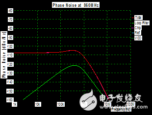
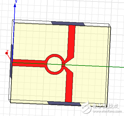
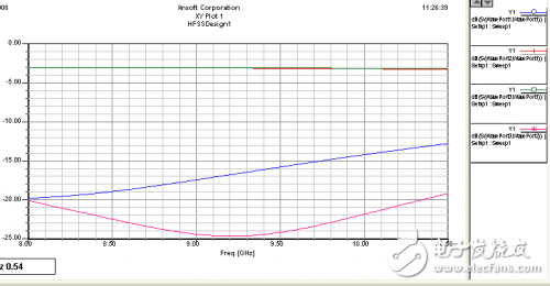
Millimeter-wave systems are widely used in radar and guidance, electronic countermeasures, millimeter wave communications, remote sensing telemetry and other fields. As a key part of a millimeter-wave system, a millimeter-wave frequency source, its performance directly affects the overall performance of the system. Direct frequency synthesis is an important way to obtain a high-performance millimeter-wave frequency source, but it is bulky, complicated, and spurious. Since the emergence of digital phase-locked integrated devices, the phase-locked frequency synthesizer has been rapidly developed, but when a narrow frequency step is required, the loop bandwidth needs to be reduced, resulting in a longer locking time and failing to meet the requirements of fast frequency hopping. The emergence of DDS can just make up for this defect, but its output frequency upper limit is too low and broadband spurious is large. In practical applications, the combination of the above methods can be used to compensate for the limitations of applying a certain method. In this paper, according to the requirements of millimeter-wave radar for frequency sources, a combination of DDS and mixing PLL is used to achieve high-resolution, low spurious signal output. This article needs to design a frequency resolution better than 1MHz, phase noise is better than -85dBc/Hz@1KHz, better than -90dBc/Hz@10KHz; spurious suppression is better than 55dBc, and frequency hopping time is better than 50 microsecond millimeter wave frequency source. The "X-band frequency synthesis + millimeter-wave quadrupling" solution is adopted. The phase noise requirement for X-band frequency synthesis is raised to -97dBc/Hz@10kHz, -102dBc/Hz@10kHz, frequency step is 0.25MHz, in-band spurious "-67dBc. In order to achieve higher X-band frequency synthesis For indicators, we will combine DDS and phase-locked loops to take advantage of DDS and PLL loops to avoid shortcomings. The introduction of DDS, and its high frequency resolution, high frequency conversion speed characteristics to ensure the system's high-resolution, agile. At the same time, the DDS output signal and the DDS reference clock signal up-conversion scheme and the mixer phase-locked loop structure introduced into the mixer in the feedback branch are used to reduce the total loop frequency divider ratio and achieve low phase noise performance of the system. The triple adjustment of the DDS frequency, reference division ratio, and loop division ratio avoids large spurious DDS frequencies. The system plan is shown in Figure 1. Fig. 1 System Scheme Diagram of Frequency Synthesizer 3.1 DDS and PLL circuit design The DDS circuit uses the AD9858 chip, which is a DDS device with excellent performance. It consists of a low-power DDS core, a 32-bit phase accumulator, a 14-bit phase offset adjustment circuit, and a 1 GSPS 10-bit DAC. This new DDS can directly generate up to 400MHz when driven at an internal clock rate of 1 GHz. And its 32-bit control word can provide 0.233Hz FM resolution. According to the index requirements of this circuit, the AD9858 is driven by a 3x frequency of the 100M reference crystal signal, and the 53-58MHz frequency band output with good spurious performance is selected, and then the 300M crystal signal is up-converted and sent to the PLL loop. The PLL module is particularly important in this circuit design. We use the ADF4153 phase-locked loop chip. For the ADF4153, the parameters used to calculate the output frequency are the input reference clock frequency, the feedback divider value (ie, the IN T value and FRAC value in the N Divider register), and the reference frequency divider value (ie, R in the R Divider register). Value and MOD value) and reference frequency multiplication value (that is, the D value in the control register). Calculated as follows: RFout = FPFD&TImes;( INT +( FRAC/MOD ) (1) FPFD = REFin &TImes;(1 +D) /R (2) Among them, RFout is the output signal frequency of VCO; REFi is the reference clock frequency of input ADF4153; MOD is the resolution coefficient, the range of value is 2~ 4095; IN T is the integral part of the feedback frequency value set up, value range 31~ 511; FRAC is the fractional part of the feedback divider value set, the value range 0 ~ MOD; D is the input reference frequency multiplier, R is the reference frequency divider coefficient, the value of the range of 1 ~ 15. Because the upper limit of the ADF4153 reference input frequency is exceeded after the DDS output signal and the 300M signal are up-converted, a separate digital frequency divider HMC394 is selected. Therefore, R in 4153 is set to 1, and D is set to 0. At the same time, in order to obtain better spurious performance, this design adopts integer frequency division, so FRAC is set to 0 and MOD is set to 2. Loop filter implementation is easier. Third-order passive loop filter design is selected. Since the resolution of this circuit is controlled by the DDS, the PLL frequency can be properly taken into account. Considering the frequency adjustment, the center frequency of the phase detection frequency is set to 20MHz. Combined with the device and engineering experience, the loop bandwidth is taken as 500KHz. Left and right, the initial value of the phase margin is set to 48 degrees. The ADIsimPLL software can easily calculate the parameters of the loop filter components. Due to the use of a frequency-mixed phase-locked loop, the 9.6G local oscillator signal is mixed with the VCO output 8.7-8.8GHz signal to obtain an 800-900M IF signal, so the loop actually locks the 800-900M signal. The PLL circuit simulation results are shown in Figure 2 below. Figure 2 Phase noise simulation As can be seen from Figure 2, the simulated phase noise results are better than the design values. 3.2 Design of microwave frequency multiplier link Due to the use of a mixed phase-locked loop structure, a 9.6GHz microwave frequency doubler link needs to be designed. As can be seen in Figure 1, the 100MHz high spectral purity crystal signal is first multiplied to 300MHz, filtered and amplified, and the power is divided into three ways. All the way to DDS reference clock, all the way to DDS upconverting the local oscillator signal, leaving the other way by 2 * 16 times Frequency chain to 9.6GHz, filter amplification to do the mixer MIX2 RF input. In order to keep signal phase noise from deteriorating greatly, in the design process of the frequency multiplication chain circuit, we first select the device with suitable performance, and secondly, we design the signal power level reasonably, and no low power point appears. Otherwise, the additional noise is introduced. Phase noise will probably dominate. Since the 600MHz signal is multiplied by 16 to 9.6GHz, a filter is added to filter out its harmonics and spurs. Therefore, a 3rd order microstrip hairpin filter filter is used for filtering. 3.3 X Band Splitter Design As can be seen from Figure 1, the VCO output signal is fed all the way to the millimeter-wave frequency multiplier. The other way is to supply the PLL with the required local oscillator signal. Therefore, the 8.7GHz-8.8GHz power divider needs to be designed. The simulation model and simulation results are shown in Figure 3 and Figure 4. As can be seen from the simulation results, the power divider performs the design task well. Figure 3 Simulation model of power divider Figure 4 Simulation results of the power divider 3.4 millimeter wave 4 times frequency circuit design Millimeter wave 4 times the frequency link part, select the millimeter wave quadrupler and monolithic amplifier amplification output. 3.5 Circuit Layout On the whole, the upper and lower sides of the cavity are double-sided boards, the front of the cavity is a phase-locked loop, DDS, power supply and control circuit, and the back is a 9.6GHz frequency-multiplying chain and millimeter wave part. In order to prevent signals from each functional module from interfering with each other, the front and rear chambers are equally spaced and isolated. This paper introduces a Ka-band frequency source scheme and circuit simulation design. This frequency source combines DDS and frequency-mixed phase-locked loops to compensate for each other's weaknesses, enabling the entire system to have narrow steps, agile frequency conversion, low phase noise, and low spurious. The characteristics.
ZGAR AZ Vape Pods 5.0S
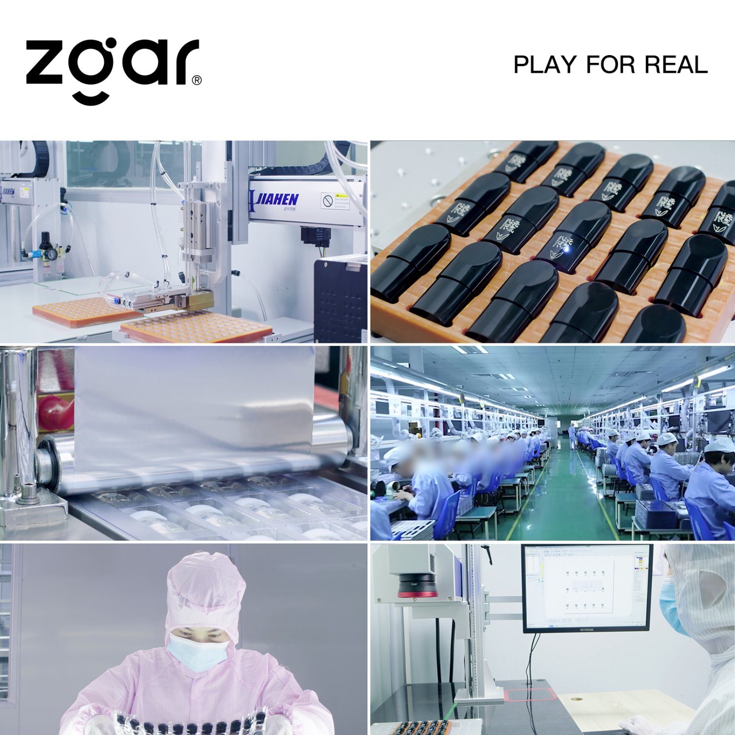
ZGAR electronic cigarette uses high-tech R&D, food grade disposable pod device and high-quality raw material. All package designs are Original IP. Our designer team is from Hong Kong. We have very high requirements for product quality, flavors taste and packaging design. The E-liquid is imported, materials are food grade, and assembly plant is medical-grade dust-free workshops.
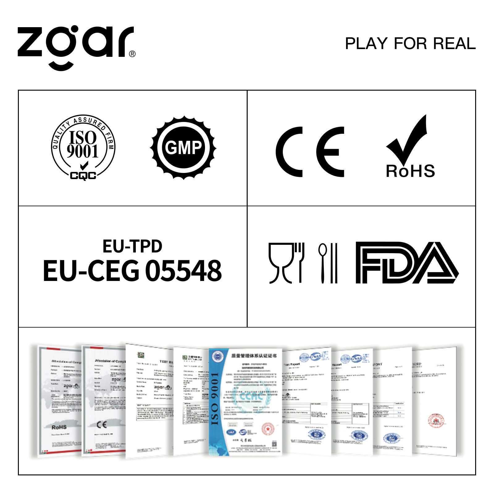
From production to packaging, the whole system of tracking, efficient and orderly process, achieving daily efficient output. WEIKA pays attention to the details of each process control. The first class dust-free production workshop has passed the GMP food and drug production standard certification, ensuring quality and safety. We choose the products with a traceability system, which can not only effectively track and trace all kinds of data, but also ensure good product quality.
We offer best price, high quality Pods, Pods Touch Screen, Empty Pod System, Pod Vape, Disposable Pod device, E-cigar, Vape Pods to all over the world.
Much Better Vaping Experience!
Pods, Vape Pods, Empty Pod System Vape,Disposable Pod Vape Systems ZGAR INTERNATIONAL(HK)CO., LIMITED , https://www.szvape-pen.com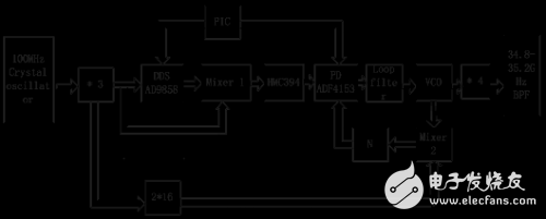
Ka-band frequency synthesizer based on DDS drive PLL structure detailed tutorial
1 Introduction