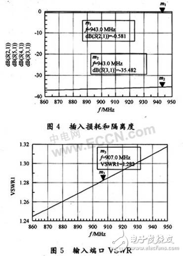
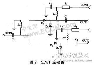
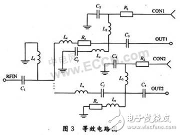
Since the receiving and transmitting frequencies of the UHF RFID are the same, the structure of the card reader is basically zero intermediate frequency structure. The receiver RF front end of the zero-IF structure has no filter selection, and the anti-interference ability of signals adjacent to the frequency is very weak. The frequency hopping interval specified by China in the "Application Requirements for Radio Frequency Identification (RFID) Technology in the 800/900 MHz Band (Trial)" is 250 kHz. This is a very good operation for RFID readers with zero-IF structure in multi-interrogator environment. Big technical difficulties. Therefore, UHF RFID readers working in the current multi-interrogator environment are basically working in time division multiplexing. Adding a single-pole multi-throw switch (Single Pole 4Throw, SP4T) to the card reader, the machine polls 4 antennas, which can replace the other 3 card readers, reducing the overall system cost. 1.1 Main technical indicators of SP4T The main technical specifications of SP4T are insertion loss, isolation, switching time, VSWR and power capacity. For the system, the SP4T is required to have a power capacity greater than 30 dBm, the control signal is a 1 kHz square wave, the insertion loss is less than 2 dB, and the VSWR is less than 1.5:1. 1.2 PIN structure and equivalent circuit The PIN tube is a non-doped intrinsic I region between the heavily doped P layer and the N layer. The true intrinsic region cannot be realized. The actually used PIN tube I region is mostly low doped. Zone N. The I region reduces the capacitance between the diode stages and increases the breakdown voltage. The wider I region increases the reverse breakdown voltage of the diode, increasing its power capacity. At the same time, the carrier transit time becomes longer, the impedance changes slowly, and the switching time becomes longer. When the area of ​​the I region increases, the on-resistance decreases, the conduction power capacity increases, the junction capacitance rises, and the cutoff frequency decreases, which limits the operating frequency and bandwidth of the system. When the PIN tube is positively biased, the microwave signal is equivalent to a linear resistance, and the magnitude of the resistance is determined by the bias current, which is close to the short circuit. In the case of reverse bias, the carrier in the I region is depleted, and the PIN tube is equivalent to a constant capacitance to the microwave signal. Its microwave equivalent circuit is shown in Figure 1. In Figure 1: Rj is the resistance introduced by the dissipation loss. Because it is much smaller than the impedance of Cj, it is often omitted; Lp and Cp are the lead inductance and package capacitance, and the presence of Lp and Cp greatly reduces the high-frequency characteristics of the circuit. Therefore, when the frequency is high, the circuit is generally built directly by the die. 1.3 SP4T circuit structure The PIN tube-based RF switching switch has a series connection, a parallel type, and a series-parallel combination. In the design, a series-parallel structure is adopted to achieve the above-mentioned index, and the basic circuit structure is shown in FIG. 2. In the SP4T, the four channels are identical, and only the first and second channels are shown in Figure 2. Among them: R1, R2 are DC bias resistors, ensuring that the PIN tube works at a proper forward bias current; C1, C3, C5 are DC blocking capacitors; L2, L3 are RF choke inductors, which together with C2, C3 form a low The network is connected to prevent the RF signal from entering the power supply; CON1 and CON2 are the switch selection control signals, and the input is a +5 V, -5 V square wave signal. When CON1 is -5 V and CON2 is +5 V, D1 and D4 are turned on, D2 and D3 are turned off, channel 1 is turned on, and channel 2 to channel 4 are turned off. The PIN tube during conduction is equivalent to a small series resistor R3, and the cut-off PIN tube is equivalent to a series connection of a resistor Rr and a capacitor Cj, so the equivalent circuit when the other channels are closed is shown in FIG. Show. 1.4 main component selection and circuit simulation Analysis circuit is available, the smaller Rs and Cj are necessary to obtain low insertion loss and high isolation, and the power capacity of the circuit is determined by the maximum reverse voltage of the PIN tube and PDM. It can be seen from Fig. 4 that the insertion loss of the closed channel is less than 1 dB between 860 and 950 MHz, and the impedance of each disconnected channel is symmetrical due to the circuit symmetry, which is greater than 34 dB. The VSWR curve of Figure 5 increases with increasing frequency, mainly due to the effect of the reverse channel junction capacitance of the open channel. For the DC bias circuit, the main reason is to ensure that the positive bias current of the PIN tube is 10 mA, and the current limiting resistor value is 500 Ω. With a control voltage of 5 V, the 10 mA operating current of the PIN tube is guaranteed. C1, C3, and C6 are DC blocking capacitors. On the one hand, the attenuation of the 860-950 MHz control signal is small, and on the other hand, the attenuation of the 1 kHz control signal is large. In order to avoid the control signal entering the rest of the system, the capacitance value here is 20 pF. C1 and L1, C2 and L2, C4 and L3 form three low-pass networks whose cutoff frequency depends on the highest frequency of the control signal. For a 1 kHz square wave signal, taking a rise time of 0.5 μs, the bandwidth is BW=1/[2*tr(10%~90%)]=1/(2&TImes;0.5μs)=1 MHz, here Take C1, C2, and C4 as 47 pF; L1, L2, and L3 are 56 nH. The low-pass network can ensure that control signals are applied to the respective PIN tubes in case the high frequency is prevented from entering the power source. Due to the low frequency of the system, considering the cost and production factors, the FR-4 board was used to complete the circuit and tested with Agilent's Network Analyzer 8712ET to achieve a maximum insertion loss of 1.42 dB and a minimum isolation of 25 dB. Compared with the simulation results, the actual test value is greatly deteriorated. The main reasons are as follows: (1) The model used in the simulation is not accurate. Since the simulation model is established based on the parameters given by the manufacturer, the parasitic capacitance and the parasitic inductance value are empirical values, which is somewhat different from the actual value. (2) Coupling between the microstrip lines of each branch. Since the common contacts of the branches are connected together, the distance between the microstrip lines is very close, and the signals of the closed channels are coupled to the adjacent two disconnected channels, which deteriorates the insertion loss and isolation of the system. (3) There are many disconnected channels of the multi-way switch. The reverse bias equivalent capacitance is connected in parallel on the closed channel, resulting in a large insertion loss, which is the main reason why the number of multi-way switches cannot be too large. The circuit in the form of a series of parallel PIN tubes is the best way to achieve high speed, wideband, multi-channel microwave switches. Through careful selection of the PIN tube and careful optimization of the circuit, the bandwidth of the system can be further increased and the insertion loss of the system can be reduced.
ZGAR Aurora 500 Puffs
ZGAR electronic cigarette uses high-tech R&D, food grade disposable pod device and high-quality raw material. All package designs are Original IP. Our designer team is from Hong Kong. We have very high requirements for product quality, flavors taste and packaging design. The E-liquid is imported, materials are food grade, and assembly plant is medical-grade dust-free workshops.
Our products include disposable e-cigarettes, rechargeable e-cigarettes, rechargreable disposable vape pen, and various of flavors of cigarette cartridges. From 600puffs to 5000puffs, ZGAR bar Disposable offer high-tech R&D, E-cigarette improves battery capacity, We offer various of flavors and support customization. And printing designs can be customized. We have our own professional team and competitive quotations for any OEM or ODM works.
We supply OEM rechargeable disposable vape pen,OEM disposable electronic cigarette,ODM disposable vape pen,ODM disposable electronic cigarette,OEM/ODM vape pen e-cigarette,OEM/ODM atomizer device.
Aurora 500 Puffs,Pod System Vape,Pos Systems Touch Screen,Empty Disposable Vape Pod System,500Puffs Pod Vape System ZGAR INTERNATIONAL(HK)CO., LIMITED , https://www.szdisposable-vape.com
![]() ,
, ![]() The minimum value in . Based on the above considerations, MA-COM's MAP4P789 and SC-79 packages were selected. The parameters are Vr=75 V, Cj=0.35 pF, Rs=1.5 Ω 10 mA, package inductance 0.6 nH, and package capacitance 0.1 pF. Substituting the above parameters into the circuit and simulating with ADS, as shown in Figure 4 and Figure 5.
The minimum value in . Based on the above considerations, MA-COM's MAP4P789 and SC-79 packages were selected. The parameters are Vr=75 V, Cj=0.35 pF, Rs=1.5 Ω 10 mA, package inductance 0.6 nH, and package capacitance 0.1 pF. Substituting the above parameters into the circuit and simulating with ADS, as shown in Figure 4 and Figure 5.