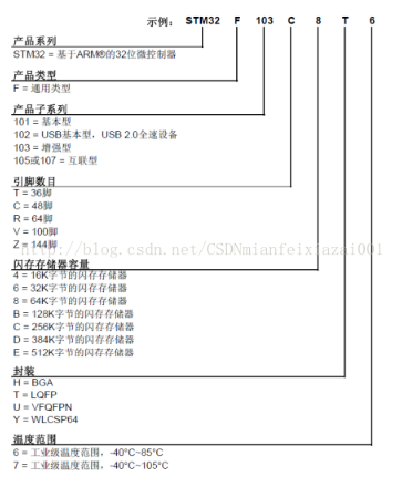
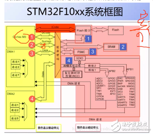
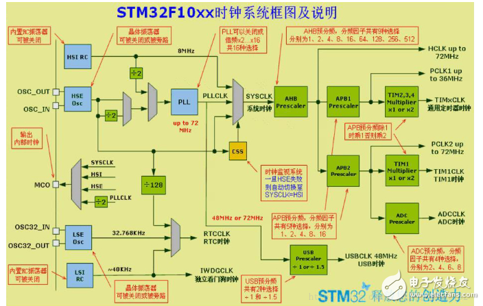
For many people who have just started to get in touch with the STM32 series of single-chip microcomputers, they may feel at a loss for this series of single-chip microcomputers. I don’t know how to distinguish between so many single-chip microcomputers that suddenly appeared. I will not say much. , Directly above: annotation: (1) STM32 refers to the 32-bit MCU (microcontroller) produced by ST (STMicroelectronics) (2) F---refers to the general product type (3) 1xx refers to the sub-series of the product (4) Package refers to the package format of the corresponding chip pin stm32 architecture One. First, let me talk about the common points and differences of the STM32F10x chip embodied by the silk screen. Let me briefly talk about the naming rules: 101 basic type, 102USB basic type, 103 enhanced type, 105 or 107 interconnected type. T: 36 feet, C: 48 feet, R: 64 feet, V: 100 feet, Z: 144 feet. C: 256K SRAM, D: 384K SRAM, E: 512K SRAM. When we are facing the silk screen of the chip, we will see a small dot (positive direction) in the lower left corner of the chip, and some have a slightly larger circle mark in the upper right corner. The pin number near the small dot in the lower left corner is 1. Then in the counterclockwise direction, the last pin number of ZET6 is 144, and the last pin number of VET6 is 100, that is, Z has more pins than V, so Z has more functions than V; Next, let’s talk about the ARM and ST on the silk screen. The crotex-Mx core was designed by ARM (called IP manufacturer). A block of 32 must have peripheral circuits in addition to the core. After ST has obtained the authorization for the ARM core design, according to This design of peripheral circuits (SOC manufacturers, like Samsung, Apple, Freescale... are all SOC manufacturers, and the cores they use are authorized by IP manufacturers), such as FLASH for storing programs, SRAM for storing variables, and external Set (GPIO, IIC, SPI, USTAR, etc.), to summarize the 32 chip architecture is composed of the core (drive unit) and peripherals (passive unit). (1) Drive unit Icode bus: After the program we have written is compiled, it will become an instruction stored in the peripheral's FLASH. The kernel must read these instructions to execute the program through the Icode bus (specially used to fetch instructions). DCode bus and DMA bus: That is DATA, we know that the constant const is stored in the internal FLASH, and the variable is stored in the internal SRAM. These data can be read by DCode and DMA. In order to avoid conflicts caused by both reading data at the same time, there will be a bus matrix to determine who reads the data when the two read data. System bus: Reading data is mainly used to access peripheral registers, that is, reading and writing registers are all done through this bus. DMA bus: Let me start by saying that this bus is also mainly used to transmit data. This data can be the data register of a certain peripheral, it can be SRAM, or it can be internal FLASH. Let’s take an example to illustrate the role of the DMA bus. There is also a simple distinction between DMA and DCode. If we don’t have DMA, we need to read a data from SRAM to the internal peripheral data register DR. First, the CPU passes DCode. The bus reads the data from the SRAM to the internal general-purpose register of the CPU to temporarily store the data, and then transmits the data to the DR through the DCode bus, thus passing the CPU as a data transfer. But we now have a DMA bus, and we can send the data in SRAM directly to DR only by sending commands from the CPU. (2) Passive unit Internal FLASH: In the internal flash memory, the program we have compiled is compiled and stored here as instructions. Crotex-Mx accesses the internal FLASH through the ICode bus to fetch instructions. Internal SRAM: Static Random Access Memory It is a kind of memory with static access function, and it can save the data stored in it without refreshing the circuit. Unlike DRAM (Dynamic Random Access Memory) that requires a refresh circuit, DRAM must be refreshed and charged every once in a while, otherwise the internal data will disappear. So SRAM has higher performance, but SRAM also has its shortcomings. That is, its integration level is low, and the DRAM memory of the same capacity can be designed into a smaller volume, but SRAM requires a large volume, so the SRAM memory on the motherboard takes up a part of the area. Of course, the advantage of SRAM is that it is fast and does not need to cooperate with the memory refresh circuit, which can improve the overall work efficiency. The disadvantages of SRAM are low integration, high power consumption, large volume with the same capacity, and high price, so a small amount is used in key systems to improve efficiency. The overheads like program variables, stack, etc. are all based on the internal SRAM, and Crotex-Mx accesses it through the DCode bus. FSMC: Flexible StaTIc Memory Controller Variable static memory controller, this is the STM32 series adopts a new type of memory expansion technology. Due to the setting of special function registers, FSMC can send out corresponding data/address/control signal types to match different external memory types. The speed of the signal, so that the STM32 series microcontrollers can not only apply a variety of different types and speeds of external static memory, but also can expand a variety of different types of static memory at the same time without adding external devices to meet the needs of system design Comprehensive requirements for storage capacity, product volume, and cost. To emphasize, only static memory can be expanded. STM32F10xx system clock tree: Let me talk about 5 clock sources first, as shown in the left part: 1. HSI is a high-speed internal clock. The frequency of the RC oscillator is 16MHz, which can be used directly as the system clock or as the input of the PLL after dividing by two. 2. HSE is a high-speed external clock, which can be connected to a 4~26MHz quartz ceramic resonator or an external clock source. It can be directly used as a system clock or used as an input to the PLL after frequency division by two. 3. LSE is a low-speed external clock, connected to a 32.768KHz quartz crystal, which is mainly the RTC clock source. 4. LSI is a low-speed internal clock, RC oscillator, about 32KHz, for independent watchdog and automatic wake-up unit. 5. PLL surrounds the phase-locked loop frequency multiplication output, 32 has two PLLs on it Rubber Pipe,Cummins Rectangular Ring Seal,Cummins O Ring Seal,Cummins Keyway Seal,Cummins Plain Hose Chongqing LDJM Engine Parts Center , http://www.ckcummins.com


Talking about the naming rules and system architecture of STM32 MCU
STM32 MCU naming rules