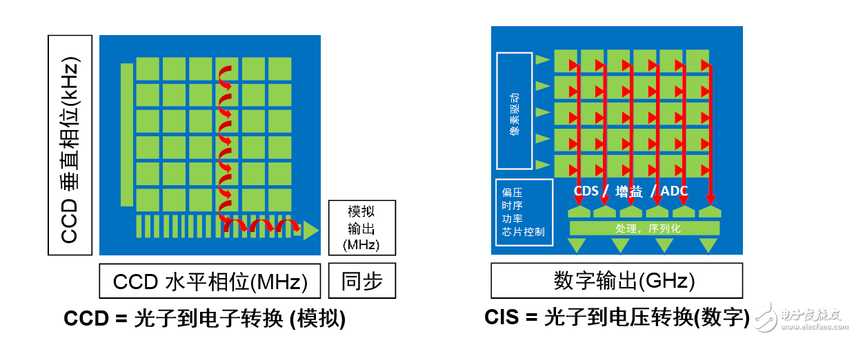
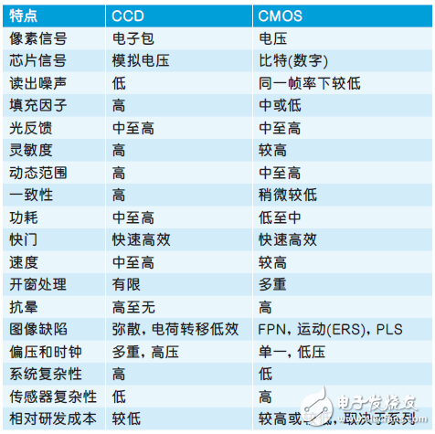
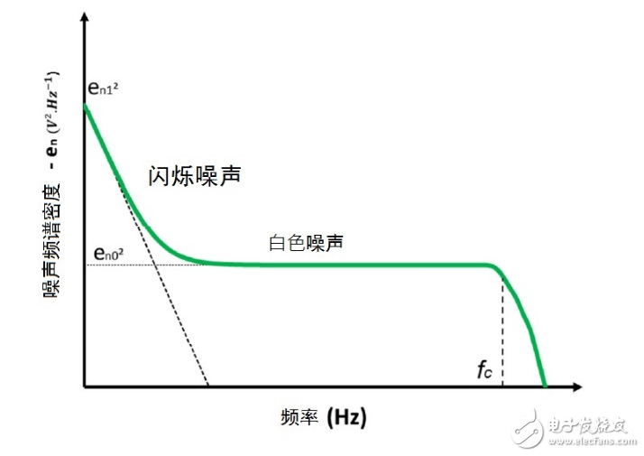
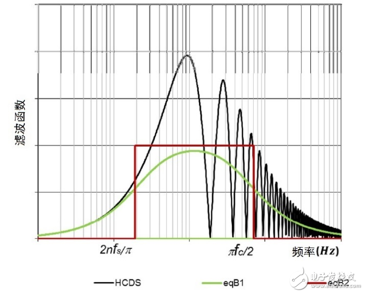
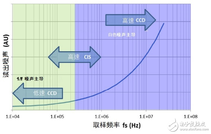
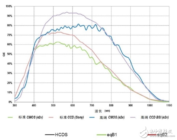
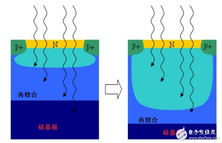
Based on Moore's Law, the shrinking of technology nodes has enabled SoC technology to rapidly expand and become more competitive from 2000. Now CIS continues to strive to improve optoelectronic performance, which is superior to CCD in many respects. If you use the "evolutionary" metaphor, you can think of CIS as a mammal that survives many natural disasters, and this evolutionary history is an epic story that spans 65 million years! As early as the early 1990s, there were opinions that the charge-coupled device (CCD) was gradually becoming a "technical dinosaur". If you look at Sony's 2015 release, this prediction seems to make sense. At that time, Sony officially announced the termination of the mass production CCD schedule and began to receive the final order. Although the industry has expected this move to happen sooner or later, the release of Sony still shocked the professional imaging community. It is worth mentioning that many industrial or professional applications - the key market for CMOS image sensors (CIS) - are still based on CCD sensor technology. What are the characteristics of CCD better than CIS, making it more attractive? In the early days of development, both CCD and CIS technologies coexisted. Later, CCDs were seen as high-end technologies capable of meeting stringent image quality requirements, while CMOS technology was still immature and subject to problems such as inherent noise and pixel complexity. During this period, image technology was still dominated by analog structures, and the concept of integrated image processing functions (system-on-chip, SoC) has not been seriously considered. Based on Moore's Law, the shrinking of technology nodes has enabled SoC technology to rapidly expand and become more competitive from 2000. Now CIS continues to strive to improve optoelectronic performance, which is superior to CCD in many respects. If you use the "evolutionary theory" mentioned in the first article, you can actually regard CIS as a mammal that survives many natural disasters, and this evolutionary history is an epic story spanning 65 million years! The CCD works by converting photon signals into electronic packets and sequentially transferring them to a common output structure, which then converts the charge into a voltage. These signals are then sent to the buffer and stored off-chip. In CCD applications, most of the functions are performed on the camera's board. When the application needs to be modified, the designer can modify the circuit without having to redesign the image chip. In a CMOS image sensor, the operation of converting a charge into a voltage is performed on each pixel. CMOS image chips convert charge to voltage at the pixel level, and most of the functionality is integrated into the chip. In this way, all functions can be operated from a single power source, and the image can be flexibly read out according to the region of interest or window opening. In general, CCDs use NMOS technology to achieve performance through specific processes such as double-layer polysilicon, anti-halation, metal shielding, and specific starting materials covering each other. CMOS is based on standard CMOS process technology for digital integrated circuits, and then incorporates imaging functions (such as embedded photodiodes) according to customer requirements. The general insight is that the production cost of a CMOS sensor is lower than that of a CCD, so its performance is also lower than that of a CCD. This assumption is based on market demand considerations, but other professional market opinions suggest that the technical level of the two is similar, and CCD may even be more economical. For example, most space programs still use CCD devices, not only because CCD can achieve performance optimization at the process level in the small batch and low cost considerations, but also the need for long-term stable supply. Similarly, high-end CCD-based solutions also have a mainstream share in the scientific imaging market, and there are some new products in the development phase. The situation is that dinosaurs have evolved into birds, and most of them provide excellent imaging capabilities... CMOS improves system complexity because it basically embeds SoC structures such as analog-to-digital conversion, correlated double sampling (CDS), clock generation, voltage regulators, or image post-processing, which were previously application systems. The function of the level design (Figure 1). Today's CIS is typically produced in a 1P4M (1-layer polyester, 4-layer metal) process from 180nm to the recent 65nm, allowing the pixel design to incorporate very high conversion factors for easy column gain amplification. This makes CMOS optical feedback and light sensitivity generally better than CCD. Compared to CMOS, the CCD chip has better substrate bias stability and fewer circuits on the chip, so it has a more significant low-noise advantage, even reaching the level of no fixed-mode noise. Figure 1: Comparison of CCD and CMOS structures. Table 1: Comparison of CCD and CMOS characteristics. On the other hand, the CIS has a lower sampling frequency, which can reduce the bandwidth required for pixel reading, and thus the instantaneous noise is also small. The shutter exposes all pixels on the array at the same time. However, if this method is used by CMOS sensors, since each pixel requires an additional transistor, it takes up more pixel space. In addition, each pixel of CMOS has an open-loop output amplifier, and the compensation and gain of each amplifier will change due to the difference in wafer process, and the brightness and darkness are worse than the CCD sensor. Compared to the CCD sensor of the same class, the CMOS sensor has lower power consumption, and the power consumption of other circuits on the chip is lower than that of the CCD optimized analog system chip. Depending on the amount of supply and considering the cost of the CCD to introduce external related circuit functions, the CMOS system cost may also be lower than the CCD. Table 1 summarizes the characteristics of CCD and CMOS. Some functions benefit one or the other, so there is no need to completely separate the overall performance or cost. However, the real advantage of CMOS is the introduction flexibility through SoC and its low power consumption. The bandwidth of the video imaging chain must be carefully adjusted to minimize readout noise during the digitization phase. However, this bandwidth must also be large enough to prevent other defects in the image. This usual practice also applies to CCD and CMOS. The minimum threshold for bandwidth is determined by the time it takes for the sample to reach a level close enough to the ideal level. The inductive error should be at a negligible level close to the least significant bit (LSB). To determine the bandwidth you need, you can apply the following guidelines: The amplification chain bandwidth fc, the signal frequencies fs and N (ie, the ADC resolution) are placed in the calculation formula. For example, when N=12, the value is: The noise is most caused by two factors: 1/f flicker noise and thermal noise (see Figure 2). Flicker noise is a common noise in nature, and its spectral density is related to the Earth's rotation speed, seabed currents, weather and climate phenomena. The study shows that the flash rate of a normal candle is 1/f. Among the elements of the MOS device and the amplification chain, the flicker noise is a defect caused by the technical process error, causing the charge to be trapped in the gate oxide. Charges enter and exit these "traps", causing the current in the transistor channel to be unstable, so it is also called "random telegraph noise" (RTS). The Lorentz mathematical model can be used to describe the resonant behavior of each "trap", and the sum of the models (that is, the sum of all the "traps" of the MOSFET channel surface range) will fully match the spectrum of the specific noise when displayed on the 1/f spectrum. density. The results show that the 1/f amplitude is inversely proportional to the surface area of ​​the MOSFET channel - not completely intuitive. Figure 2: Spectral noise density. To remove or reduce amplifier common-mode differences on CIS, floating-point reset noise and even transistor technology dispersion, video channels typically integrate a correlated double-sampling (CDS) stage. This element converts the video signal transfer function according to the following formula: In the formula, fs is the sampling frequency and n is the CDS factor (usually n=2). As shown in Figure 3, depending on the sampling frequency, this filtering can remove the 1/f noise frequency component more or less, especially when the sampling frequency fs is high (in other words, the charge in and out of the "trap" action). Will be slower than the CDS frequency). The low pass filter of the HCDS filter combined with the amplification chain can be simplified to an equivalent band pass filter as shown in FIG. The eqBP1 in the figure corresponds to a first-order bandpass filter. Here the noise spectrum function of eqBP1 is divided by 2 to obtain an equivalent integrated noise power with an HCDS function. eqBP2 is the notch estimate for eqBP1. To achieve integrated noise power, the upper and lower limits of eqBP2 are multiplied by (π/2)-1 and π/2, respectively. Figure 3: Noise filter function. In the general situation shown in Figures 2 and 3, the noise performance can be shown in the following equation: After combining equations (1) and (4), the estimated values ​​of the overall integrated readout noise are as follows: The calculations are verified to match the numerical simulation results. The readout noise of the CCD can reach very low levels, suitable for astronomical or scientific imaging, and the readout frequency of these applications can be very low. The system design contains electronic elements with minimal bandwidth to avoid integration into the unstable clock of the signal. In these applications, the 1/f component of the noise dominates (Figure 4). In high speed video applications, high noise makes the signal to noise ratio significantly worse. The specific noise representation status data recorded from a number of different CCD video cameras confirms the theory. The columnar parallel readout layout of the CMOS image sensor (see Figure 1) provides advantages in this regard. The threshold readout frequency is divided by the number of columns and compared to the CCD value. Here, the read noise of the CIS is mainly dominated by the 1/f value. This helps to further improve the imaging performance of CMOS technology. Recent results show that CIS offers excellent noise performance in the 1e- or lower range. Figure 4: Read noise as a function of fs. Quantum efficiency (QE) is a factor that directly affects the optoelectronic performance of an image sensor because any loss in photoelectric conversion efficiency directly reduces the signal-to-noise ratio (SNR). Its effect is two-fold, because when shot noise (the square root of the signal) is the main source of noise, QE is not only the divisor (signal) of the signal-to-noise ratio, but also the divisor (noise). Above this point, CCD and CMOS are at the same level, but CCD has accumulated many years of technical process optimization in QE improvement, and the development of QE in CIS is relatively late. Based on the physical properties of the silicon species, longer wavelengths can penetrate the photosensitive transition region, so thick epitaxial materials are used to increase the QE of the red and near infrared wavelengths. According to Bill Lambert's law, the absorbed energy is exponentially related to the thickness of the medium. High-end applications CCDs have advantages by using thicker silicon and back-illuminated (BSI) processes to restore high-bandwidth QE and near-infrared (NIR) sensitivity. Figure 5: QE indicator. Interlaced CCD (ITCCD) is based on a specific production process that introduces so-called "vertical spill" (VOD) or "vertical anti-halation" (VAB) functions. VAB was developed in the early 1980s with very good performance, but the disadvantage is that it reduces the red feedback and rejects the NIR part of the spectrum. Figure 6: Deep depletion method. Therefore, ITCCD cannot benefit from BSI. The high-end CCD does not have this limitation because it uses a vertical anti-halation process. What is the Patch Panel? Why is the good
choice for your Server Center and Data Center?
A patch panel is a steel panel with a
number of ports helps organize a group of cables. Each of those ports includes
a wire that goes to a different location. Patch panel could be small size with
2 ports, or very large size with hundreds of ports. They could also be
installation for fiber optic cables, RJ45 cables, CAT5E / CAT6 / CAT6A/ CAT7 /
CAT8 Ethernet cables, and many others.
CAT6 Patch Panel,patch panel cat6,10 Inch 1U Patch Panel,Home Network Patch Panel NINGBO UONICORE ELECTRONICS CO., LTD , https://www.uniconmelectronics.com