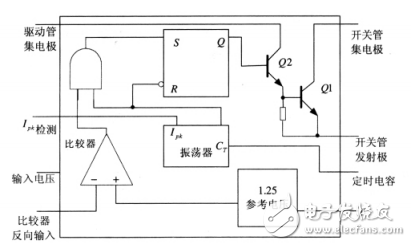
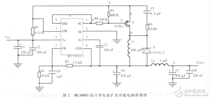
Abstract: The MC34063 is used to design a negative power supply circuit with current expansion. The power MOS tube NTB2506 is used as an external switch tube. By adjusting the gate drive resistance of the power MOS transistor and the resistance between the gate and the source, the gate has an optimal driving voltage waveform. And current size to increase the output power and efficiency of the power supply. Experiments show that the designed power supply output current can reach 1A, and the volume is small and the efficiency is high. In the development of interferometric fiber optic sensors, phase carrier (PGC) modulation and demodulation is a commonly used signal detection scheme. It consists of a filter circuit, an analog multiplier, a D/A conversion circuit, a differential circuit, an integration circuit, etc. Power is supplied and requires a large amount of power. If the system is powered by a linear power supply scheme, it is necessary to generate two positive and negative DC voltages through buck, rectification and filtering, and then use a voltage regulator chip for voltage regulation, which is not only inefficient, but also the filter capacitor and heat sink increase the volume of the power supply. Not suitable for the requirements of circuit miniaturization. When the power supply is switched by the switching power supply scheme, only one set of DC voltage after step-down rectification by the transformer is needed, and a regulated power supply with various output voltages can be designed, and the power density is high and the heat generation is small. In the switching power management chip, the output is a positive power supply with many types of devices, the circuit is easy to design, and the power supply circuit whose output is a negative power supply and whose output current reaches 1A is difficult to design. In this paper, MC34063 is used to design the negative power supply circuit, NTB2506 is used as the external power tube, and the gate drive waveform is optimized to improve the output current of the power supply. The internal block diagram of the MC34063 is shown in Figure 1. It is a monolithic bipolar integrated circuit with the main functions required by the DC/DC converter. The reference voltage generator, comparator, and duty cycle controllable oscillator. , RS trigger and high current output switch tube and other components. Figure 1 MC34063 block diagram MC34063 circuit control mode is its excitation type, there is an internal oscillator, through the external capacitor, generate a certain frequency of the switching pulse signal to control the disconnection of the switch tube, so that the output has a stable DC voltage output, the switching frequency is external capacitor Decide. MC34063 can complete various voltage conversion functions according to actual needs. The working principle of the voltage regulator circuit is as follows: When the output voltage is lower than the specified value of the design, the input voltage of the feedback terminal is less than 1.25V of the internal reference power supply, the error comparator outputs a high level, and the "AND gate" is turned on, and the oscillation pulse of the oscillator is added to the RS. The R terminal of the flip-flop causes the output terminal Q to be high level, the switch tube is turned on, and the input voltage is charged to the filter capacitor, so that the output voltage rises until the feedback voltage is equal to 1.25V of the internal reference power supply, the circuit reaches an equilibrium state, and the output The voltage is stable at the value specified in the design; conversely, when the output voltage is higher than the specified value, the switch is turned off, the capacitor is discharged, the output voltage is reduced, and finally the value specified in the design is stabilized, thereby achieving the purpose of voltage regulation. The MC34063 switching power supply controller is a single-ended output DC converter that can not only design step-up and step-down circuits, but also perform voltage inversion functions [3]. When designing the negative power supply circuit with voltage inversion, due to the internal circuit structure of the chip, the current flowing through the switch tube is trapezoidal, and the efficiency is low. When the output current exceeds 200mA, the power supply system is unstable and the output ripple is unstable. The voltage is increased, which cannot meet the requirements of large load requirements, which seriously affects the application range. The negative power supply circuit with current expansion using MC34063 is shown in Figure 2. The choice of external switch tube has a great influence on the circuit performance, which directly determines the size and efficiency of the output current of the circuit. The triode is used as an external switch, which can be connected to the internal power tube into a Darlington form and a non-Darlington form. When a non-Darlington circuit is used, during the switching process, the base of the triode stores charge, which causes the tube to reach saturation. When the deep saturation is reached, the switching frequency is affected, which limits its application range. When the Darlington circuit is used, although the charge saturation phenomenon does not occur, the voltage drop increases when the switching tube is turned on, the power consumption is significantly increased, the triode heat is severe, and the output current is limited. There are many advantages when using a power MOSFET as an external switch. It is a unipolar voltage control device with majority carrier conduction. It has no charge storage problem, and has fast switching speed, high frequency performance, high input impedance, low driving power and no secondary breakdown. [5 ]. The NTB2506 is a P-channel power MOSFET with high-speed switching characteristics under low-voltage conditions. It has good switching characteristics and low loss. Its drain and source withstand voltage is 60V, and the gate and source voltages can reach 20V. Current can reach 27.5A. Therefore, this paper selects NTB2506 as the external switch tube and the power tube inside MC34063 and connects it into the non-Darlington form circuit structure. The gate drive waveform of the power MOSFET has an important influence on the efficiency of the power supply. If the R5 and R6 values ​​are not properly selected, the power supply efficiency will be low, the power tube will be hot, and the output current will be reduced. The requirements of the power MOSFET for the gate drive circuit are: optimal drive voltage and current waveform, optimal drive voltage and current [6]. The resistor R5 is applied between the gate and the source, and the main function is to charge the equivalent capacitance between the gate and the source of the power MOSFET through the resistor, improve the waveform of the driving voltage, and ensure that the turn-on signal has a good leading edge steepness. If the value of R5 is too large, the sudden change in voltage between the drain and the source will be coupled to the gate through the inter-electrode capacitance, resulting in a relatively high gate-source spike voltage. The light voltage will cause the power MOSFET to be severely heated. This will cause the gate-source oxide layer to break down, causing permanent damage to the tube. The resistor R6 is a gate driving resistor for adjusting the magnitude of the driving current and the waveform of the driving voltage. When the power MOSFET is turned on, the gate capacitor is charged with a low resistance; when turned off, a discharge loop is provided for the gate charge to increase the switching speed of the power MOSFET. The specific value of the resistor needs to be debugged by the test under the operating state of the system, so that the gate driving effect is the best. Under normal circumstances, the resistance value cannot be too large. In addition, the circuit has an inductive load. When the device is in the process of switching, the sudden change of the drain current will generate a high peak voltage, which may cause breakdown of the device. The higher the switching frequency, the greater the overvoltage generated. In this paper, two methods are used to eliminate the drain spike voltage: one is to use diode D to provide a discharge loop for the current during the NTB2506 switching process; the other is to use the resistor R4 and capacitor C4 to form an RC snubber circuit to absorb the transient between the drain and source of the NTB2506. The voltage spikes, which virtually eliminate the spike voltage, protect the power MOSFET well.
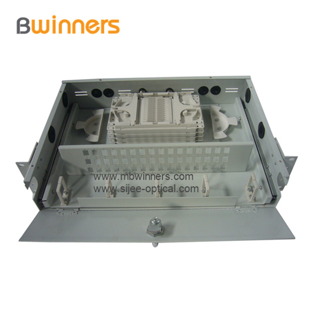
Fiber Optic Patch Panel, Termination Box Fiber Optic Termination Box/Patch Panel(OTB)designed according to the standard 19-inch cabinet, it is made of cold rolled steel of high grade and welded in its entirety with goods appearance, cabel can enter from the left or right side .
Fiber Optic Termination Box/Patch Panel(OTB) perform fiber splicing, distribution, termination, patching, storage and management in one unit. They support both cross-connect and interconnect architecture, and provide interfaces between outside plant cables and transmission equipment.
Fiber Optic Patch Panel,Fiber Optic Distribution Panel,Fiber Optical Patch Panel Sijee Optical Communication Technology Co.,Ltd , https://www.sijee-optical.com