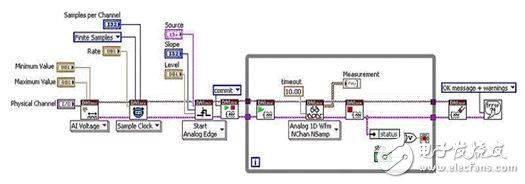
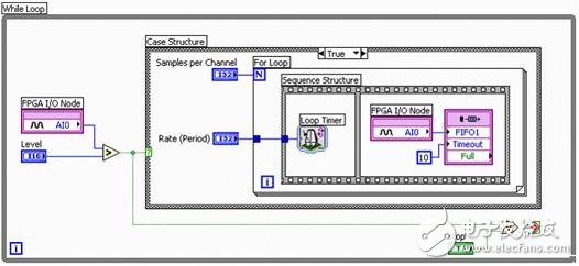
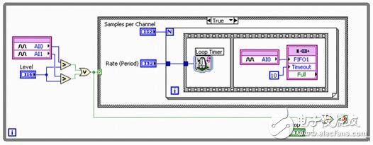
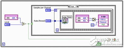
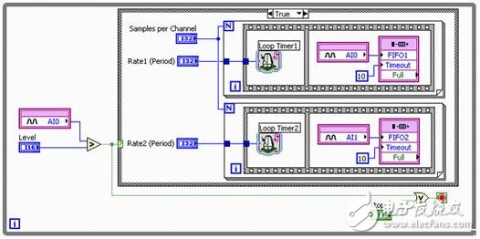
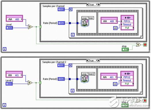
The versatile intelligent DAQ device is equipped with custom onboard processing to maximize flexibility for system timing and triggering. Unlike fixed ASICs that control device functionality, Smart DAQ uses an FPGA-based system timing controller that allows all analog and digital I/O to be configured for specific application operations. This guide shows how to perform data acquisition tasks flexibly with the R Series Intelligent DAQ Board and NI LabVIEW FPGA. The NI LabVIEW FPGA Module helps developers of DAQ systems to flexibly program applications for a variety of input/output operations. Users can embed LabVIEW code into the FPGA chip and gain the speed and reliability of hardware timing without having to know the hardware design tools such as VHDL in advance. Let us first cut into the topic from the common components of data acquisition hardware. Assuming you have an analog-to-digital converter (ADC), a digital-to-analog converter (DAC), and a digital input/output line, all I/Os are subject to some form of timing and control based on actual operation. Typical multi-function data acquisition devices use a full-featured ASIC to meet most functional requirements. For example: M series DAQ devices control the timing and triggering of various hardware components through DAQ-STC2. Intelligent DAQ hardware (eg, R-series DAQ devices) is different from any other data acquisition device on the market because intelligent DAQ replaces traditional ASICs with FPGA-based system timing controllers in terms of control device functionality, enabling all analog and digital I /O can accept the appropriate configuration according to the specific application operation. The reconfigurable FPGA chip is programmed with the NI LabVIEW FPGA Module, and the NI LabVIEW data flow mode is still applicable, but a new set of functions is used to control the lowest level of device I/O. The LabVIEW FPGA I/O Node is not responsible for implementing common tasks and functions through the NI-DAQmx functions, but is flexible to run at the lowest level of each channel. Through the following sections, we will learn about specific examples of NI-DAQmx and learn how to customize various data collection tasks with intelligent DAQ. Intelligent DAQ for advanced data collection is primarily used for custom timing and triggering. The sample block diagram below shows the triggering analog input tasks that NI-DAQmx helps implement. Figure 1. Triggered analog input via NI-DAQmx As shown in Figure 1, the intelligent DAQ does not use different functions to configure the channel. Instead, it reads and writes the analog and digital channels through a function called an I/O node. Let's take a look at the same features that are obtained using I/O nodes in NI LabVIEW FPGA. Figure 2. Triggered analog input via Smart DAQ and NI LabVIEW FPGA The above figure has no configuration functions for global channels, sample clocks, triggers, and no tasks such as start, stop, and clear. All content is replaced by a simple analog I/O read; all timing is controlled by the local LabVIEW structure (eg, While Loop and Conditional Structure). Since the entire block diagram is executed within the FPGA hardware, the LabVIEW code runs to reflect the speed and reliability of the hardware timing. Let's take a closer look at how this block diagram works. The analog I/O nodes do not specify a sample rate, but use the For loop to acquire individual samples. The corresponding ADC is responsible for actually digitizing the input signal when the I/O node is called, thus accepting timing through the For loop. If you want to sample the signal at a frequency of 100 kHz, the delay for the loop must be set to 10 μs. The cyclic timer function ensures a specific time delay from the second iteration of the loop, and the user is thus able to ensure that there is a specified time interval between the samples through the sequential structure. The powerful conditional structure in NI LabVIEW FPGA actually represents the hardware trigger used to encapsulate various types of code. Since all functions and structures are run in hardware through the logic unit, the conditional structure ensures that samples with real-time 10 μs time accuracy are started. Finally, it should be pointed out that since the operation is located at the hardware layer and only involves several levels of abstract processing, the user does not need to clear the task ID or release the memory. For FPGA-based intelligent DAQ hardware, the real advantage is the ability to customize all types of timing and triggering, and to perform signal processing and decision making in hardware. Now let's take a look at what changes to the analog input trigger are required for a particular type of custom application. If we want to trigger the acquisition when the voltage of one of the two analog input channels exceeds the specified range, how can we modify it? With NI LabVIEW FPGA, the execution of such tasks is a breeze. Figure 3. Custom Trigger Analog Inputs with Smart DAQ and NI LabVIEW FPGA Here, we have added a second I/O node and a second comparison function to the block diagram, as well as a Boolean "or" function. The intelligent DAQ hardware provides a dedicated ADC for all analog input channels, so two channels can accept simultaneous sampling; at the same time, as long as the voltage of any one channel exceeds the specified range, the conditional structure will perform a "true" condition and start with 10 The μs time precision is sampled. Keep in mind that the lack of intelligent DAQ makes it impossible to generate similar triggers; when applied on other DAQ hardware, the trigger requires software timing with higher latency. If we want to extend the monitoring range from 2 channels to all 8 channels by extension, and even want to add digital triggers, we need to simplify the custom code. After adding a pre-trigger scan, the user can continuously sample the input channel and transfer the data to the FIFO buffer. Once the flip-flop accepts the read, the FIFO buffer and subsequent samples can be transferred to the host via the DMA channel. If we want to sample the second analog input channel with the NI-DAQmx driver, the block diagram is similar to the one shown in Figure 1. However, the limitation still exists because both channels are forced to reference the same trigger and sample at the same clock frequency. Now let's take a look at the various multi-channel sampling that Smart DAQ and NI LabVIEW FPGA help. Figure 4. Triggered synchronous analog input via intelligent DAQ Figure 4 (top) shows how to simultaneously sample two different analog input channels based on the analog flip-flops in analog input channel 0. Since intelligent DAQ devices are equipped with separate ADCs, two channels in the same I/O node can be sampled at exactly the same time. A typical multifunction DAQ device can multiplex all channels through one ADC, so each channel must share the same sample clock and trigger line. Figure 5 (below) shows that intelligent DAQ hardware can actually sample different analog input channels at an independent rate. After placing the analog input I/O nodes in a separate loop, each channel is sampled at a completely different rate and then read and write to the hard disk through two DMA channels. Figure 5. Triggered multirate analog input via intelligent DAQ Finally, it should be pointed out that if we want the 2 channels to have independent sampling rates and start triggering, then we can deploy all I/O nodes in the parallel loop structure with reference to Figure 6. This approach takes full advantage of the parallelism of the FPGA, ensuring that each task can use dedicated resources and is completely independent of other acquisition tasks when executed. Figure 6. Independent Triggered Multirate Analog Input via Smart DAQ CIXI LANGUANG PHOTOELECTRIC TECHNOLOGY CO..LTD , https://www.cxblueray.com