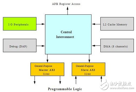
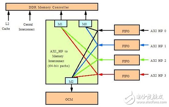
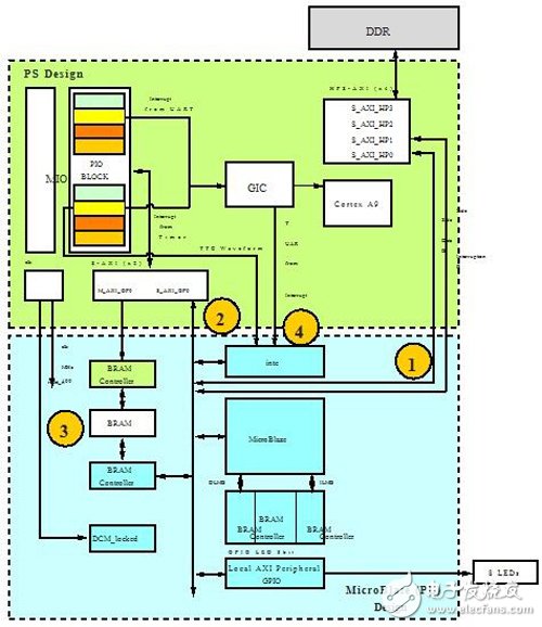
The Xilinx Zynq-7000 All Programmable SoC has a strong onboard processing capability. But the presence of the powerful dual Cortex-A9 processor and associated peripherals in the Zynq Application Processing Unit (APU) does not prevent you from adding one or more MicroBlaze processors to the same package, as long as the application benefits. Why add MicroBlaze to a solution that already has a powerful processing power? The first is the issue of reliability. Single threading will greatly improve reliability. You can place one thread per Cortex-A9 for compute-intensive tasks, and you can instantiate any number of MicroBlaze processors for other threads as needed. Secondly, you can hand over any chores to MicroBlaze to complete the work that is most needed for the powerful Cortex-A9, to make the most of its work, and save several key work cycles. The following example can reflect the above two situations. Imagine a task that requires long-term, high-intensity calculations while monitoring user input. Here, MicroBlaze manages user input (lower frequency, less computationally intensive) and writes to the APU memory space so that when the APU is idle (that is, when the processing task is completed), you can see what information needs to be processed next. Once you decide to add a MicroBlaze processor to your Zynq-based design, you'll see some problems right away. The first issue is how the APU communicates with MicroBlaze and which processor system (PS) resources are available to MicroBlaze. Many development boards, including the ZC702 and Zedboard, map many peripherals directly to the pins that are connected to the processing system. In Programmable Logic (PL), these pins cannot directly access MicroBlaze. The processing system also contains a variety of different timers and interrupt resources. Is there any way to access these resources from the MicroBlaze domain? Interface between PS and PL The tight integration of the processor system and programmable logic means that there are multiple tightly integrated connections between the Cortex-A9, the Snoop Control Unit (SCU), PS peripherals, clock management, and other functions and programmable logic. In fact, there are 6 different types of interconnections between PS and PL, and you can combine these interconnection types with each other. In addition, many paths are symmetrical, meaning that the PC can initiate a connection to the PL and the PL can initiate a connection to the PS. Figure 1: Is the boundary between PS and MicroBlaze in PL a piece of minefield? Can the two share resources? Xilinx's current application guides, user guides, and white papers provide an overview of how the Zynq-7000 APU, the "core" of design, uses programmable logic to access memory, PL-based peripherals, and hard-chip peripherals ( Such as PCIe module, BRAM, DSP48 and gigabit transceivers, etc.). To analyze how MicroBlaze is the dominant in its own domain, the logical first step is to look at the six interface variables, starting with the three types of AXI interfaces: general purpose, high performance, and accelerator coherency ports. The PS has two main AXI channels connected to the PL and two slave channels activated by the PL (Figure 2). The term "master" here means that the AXI channel is the initiator and can initiate data exchange, while the "slave" can only be used to respond to the arriving data. The main AXI channel is typically used to communicate with peripherals in the PL. The AXI channel is responsible for responding to PL requests, which may include transactions performed by the MicroBlaze processor. These AXI channels are connected to the central interconnect of the PS and can be routed to many resources. In addition, there are four high performance (64-bit wide) AXI channel connection points. From the PS point of view, all four channels are slave channels connected to the memory interface subsystem in the PS (Figure 3). The purpose of these four channels is to enable the master device in the PS to initiate DDR memory transactions. This memory interconnect and DDR memory controller is the gateway to all resources to DDR memory. Although the Cortex-A9 processor typically has a higher priority than the AXI connection, each of the four AXI connections has a "call me now" signal that gives the channel that made the request a priority. When the signal is not asserted, the architecture uses a round-robin mechanism to determine which requestor has access to a particular type of memory. The Accelerator Consistency Port (ACP) is another PL 32-bit AXI PS slave connection. The ACP is unique in that it is directly connected to the SCU. The task of the SCU is to ensure consistency between L1, L2 and DDR memory. With ACP, you can access the cache memory of each Cortex-A9 processor in the PS without worrying about data synchronization with the main memory (the hardware will handle this automatically). This feature not only greatly reduces the design burden, but also significantly speeds up data transfer between the processor and the PL. Figure 2: Simplified connection to the central interconnect of the processing system Figure 3: Simplified connection to DDR memory controller and on-chip memory (OCM) In addition to AXI links, scalable Multiple Input Output (EMIO) signals can also be used to route many PS hard peripherals up to PL for access to package pins. Only 54 package pins are directly connected to the PS, but the PS's hard peripherals can use up to 54 pins. EMIO is the channel between the PS hard peripheral and the PL. These I/O signals can be routed directly to the package pins available to the PL, and you can use these pins to communicate with PL-compatible peripherals. Additional miscellaneous signals between PS and PL can be divided into five basic classes: clock and reset, interrupt signals, event signals, idle AXI and DDR memory signals, and DMA signals. * Clock and Reset: PS provides 4 independent programmable frequencies for the PL. Usually one of these clocks is used for AXI connections. Each clock domain has its own domain reset signal that resets any device associated with that domain. * Interrupt Signal: The General Purpose Interrupt Controller (GIC) in PS is responsible for collecting interrupts for all available sources, including all interrupt sources for PS peripherals and 16 "peripheral" type interrupts for programmable logic. In addition, there are 4 direct interrupts connected to the CPU (IRQ0, IRQ1, FIQ0 and FIQ1). A total of 28 interrupts from the PS peripheral are available to the PL. * Event signal: These "out-of-band" asynchronous signals illustrate the special case of PS. The PS provides a series of signals to indicate which CPU is entering standby mode and which CPU has executed the SEV ("send event") instruction. The PS available event signal wakes up from the WFE ("Wait Event") state. * Idle AXI and DDR Memory Signals: The PS's idle AXI signal is used to indicate that there are no unprocessed AXI transactions in the PL. This signal is driven by PL and is one of the conditions used to initiate the PS bus clock shutdown function, ensuring that all PL bus devices are idle. The DDR emergency/arbitration signal is used to arbitrate to the four AXI ports of the PS DDR memory controller to indicate that the critical memory is in a tight condition. * DMA signal: The direct memory access (DMA) module of the PS communicates with the PL slave device via a series of "request and acknowledge" signals. Figure 4: Block diagram of the hardware design example Interface Drivers Receivers Transceivers Shenzhen Kaixuanye Technology Co., Ltd. , https://www.iconline-kxy.com


