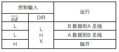
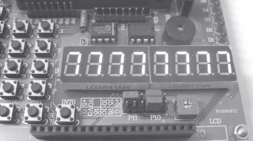
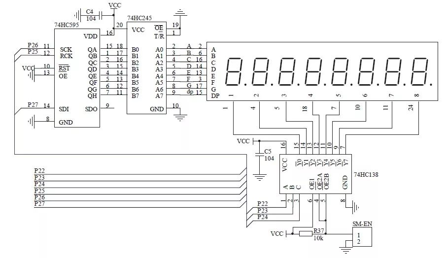
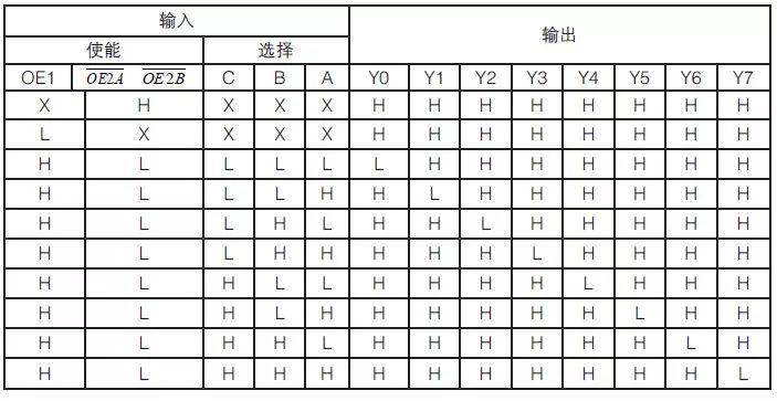
First, the content of this article The principle of the external keyboard of the SCM is introduced, and an application example is given. In this issue we will introduce the single-chip microcomputer dynamic driving segment digital tube. Through this lecture, the reader can grasp the working principle of the segmented digital tube and how to design the circuit and program through the dynamic driving method. Second, the principle of introduction The commonly used segment type digital tube has seven stages and eight stages. The eight stages have one more decimal point than the seven stages. Others are basically the same. The so-called segments are the corresponding number of small LED light emitting diodes in the index code tube, which display different fonts by controlling the on and off of different LEDs (see Figure 1(a)). From the light-emitting diode electrode connection can be divided into common anode and common cathode two types. The common cathode is that the cathodes of all the diodes are connected together, while the anodes are separated (see Figure 1(b)); while the common anodes are where the anodes of all diodes are connected in common and the cathodes are separated (see Figure 1 ( c)). The learning board uses an eight-segment common cathode digital tube, model LG3641AH. Figure 1 Internal structure of the digital tube As mentioned above, the digital tube and the light emitting diode have the same working principle. When the common anode is used, all the positive terminals are connected to the positive terminal of the power supply. When the negative terminal has a low level, the current flows through the segment, the light emitting tube is on, and the negative terminal is a high power. Normally, no current flows through the segment and the LED does not light up. To display what number, make the corresponding segment low (see Table 1). The common cathode and the common anode have the opposite state of level change. When the driving current of each segment is 2~20mA, the larger the current, the brighter the light emission. Table 1 shows the correspondence between the numbers and the seven-segment code. The commonly used seven-segment digital tube hardware driver design methods are: static drive and dynamic drive. Static drive means that each data line of the digital tube has a separate data latch. The data input by the data latch is controlled by the enable terminal. When the enable terminal is high, the data on the data line is The displayed seven-segment code) enters the display. The enable terminal is connected to the output of the address decoder. To display that bit, the address is strobed. The software design does not require a program loop, nor does the display digit flash. . But this will take up a lot of lines. The dynamic display is to connect the segment selection lines of all the digital tubes in parallel. The bit selection line controls which digital tube is valid. In this way, there is no need for each digital tube to be equipped with a latch, thereby saving the portlines and simplifying the hardware circuit. The so-called dynamic scanning display that turns to each digital tube to send out the font code and the corresponding position selection, the use of LED afterglow and persistence of human visual effects, make people feel as though everyone digital display at the same time. Third, the circuit detailed The circuit diagram is shown in Figure 2. As can be seen from Figure 2, eight eight-segment digital tubes are used to drive a total of six MCU ports, of which three IOs are controlled by the 74HC595 to drive each segment of the digital tube, and the other three IOs are controlled by the 74HC138. Realize the common drive in 8 digital tubes. In addition, in order to increase the drive capability of the 74HC595 output, a 74HC245 chip is connected after the output to increase the drive capability and increase the brightness of the digital tube. Here are three chip descriptions. Figure 2 digital tube dynamic drive circuit diagram The 74HC138 is a commonly used 3-8-wire decoder with 3 inputs (pins 1, 2, 3) and 8 outputs (pins 15, 14, 13, 12, 11, 10, 9, 7 ), The role is to complete the decoding of 3-bit binary data to 8-bit chip select. In other words, the 3 inputs correspond to 8 binary data (000, 001, 010, 011, 100, 101, 110, 111). For each input data, the corresponding bit at the output outputs low level and the other 7 bits output high level. The 74HC138 has two low-level enable pins (pins 4, 5) and one high-level enable pin (pin 6). When the low level is enabled, the low level is enabled and the high level is enabled. The 74HC138 can work normally when connected to a high level, otherwise all the 8 outputs will output a high level. Therefore, set a jumper on the learning board, as shown in Figure 2 in the SM-EN short circuit block, jump to indicate that the low level, 74HC138 normal work, jump to open the high level, 74HC138 does not work . The truth table of the 74HC138 is shown in Table 2: H represents a high level, L represents a low level, and X represents an indefinite state. Table 2 74HC138 input and output truth table The 74HC595 is an 8-bit serial input/output or parallel output shift register chip that can convert serial data to parallel output. This saves the controller's IO port resources and is therefore widely used. The 74HC595 requires up to five control lines, namely SDI (Pin14), SCK (Pin11), RCK (Pin12), The 74HC245 is an eight-bus transceiver chip that can transfer data from the A bus port to the B bus port, as well as from the B bus port to the A bus port. The direction of transfer is determined by the logic level of the DIR (chip 1 pin) input to the direction control pin. Its truth table is shown in Table 3: Table 3 74HC245 input and output truth table H represents a high level, L represents a low level, and X represents an indefinite state. Fourth, program design The core program of this tutorial design example is as follows: ...... #define SDI P2_7 (1) #define SCLK P2_6 (2) #define RCLK P2_5 (3) ...... Void dat_in(unsigned char dat) (4) { Unsigned char i; ( 5) For(i=0;i<8;i++) (6) { SCLK=0; (7) SDI=dat&0X80; (8) Dat"=1; (9) SCLK=1; (10) } RCLK=0; ( 11) RCLK=1; ( 12) } Detailed description of the program: (1) Define the data output as P2.7 pin. (2) Define the data clock output as P2.6 pin. (3) Define the register clock output as P2.5 pin. (4) Data is passed into the function, passing a byte. (5) Define an unsigned character variable. (6) Eight times because eight bytes are to be transmitted. (7) The data clock is output low first. (8) Let the data pin output the highest bit of the incoming byte. (9) The incoming byte is shifted left by one. (10) The data clock output is high and the rising edge stores the data in the 74HC595 data register. (11) The register clock is output low first. (12) The register clock output is high and the rising edge stores the data in the 74HC595 data register. The role of the above word program, when sending a byte of display data, through the 74HC595 serial to parallel control, each time sent from the microcontroller IO 1Bit out, cycle 8 times to complete sending a byte, after the output The end is transmitted to the digital tube in one byte to realize the display. V. Debugging points and experimental phenomena Connect the hardware circuit and generate the program by cold start. After the hex file is downloaded to the MCU and the MCU is reset, it can be observed that the eight digital tubes on the board are lit (see Figure 3), and the flashing changes from the digits 0 to 9. When debugging, it should be noted that the enable control terminal of the digital tube (see Figure 2) must jump with a jumper cap to allow the 74HC138 to work. It is not necessary to use the digital tube, otherwise, it is opened to save system current consumption. Figure 3 digital display effect In addition, in the dynamic scanning process, the luminance displayed by the digital tube is related to the driving current, the lighting time, and the off-time, so the size of the driving current and the scanning frequency should be properly adjusted so as to control the required brightness of the display. This is especially true when driving large-sized digital tubes. In order to stabilize the display, the hardware must achieve this driving ability, such as accessing the Linton tube again at the drive end. On the software side, constant attempts should be made during the actual debugging process (see the empirical values ​​of the number of scans in this program) to find the best critical point, that is, to pay attention to the delay interval and the number of scans of the dynamic scan. Sixth, summary This lecture introduces the principle of the single-chip microcomputer dynamic driving digital tube and gives examples. Through this lecture, we can summarize as follows: The advantages of dynamic scanning and driving the digital tube: When the number of display digits is large, the dynamic display mode is used to save the I/O port, and the hardware circuit is also more simple than the static display. Disadvantages: Its stability is not as good as the static display mode. In addition, when the number of displayed digits is large, the CPU needs to scan in turn, occupying more CPU time. In general, whether it is dynamic or static display, the display update rate can not be too fast, such as data constantly changing, too fast can not clearly see the displayed content, in the software design must pay attention. In addition, under the same conditions, the dynamic display brightness is worse than the static display, so in the appropriate increase in the drive current, for example, the use of current limiting resistors, should be slightly less than the static display circuit, or use a buffer driver chip. Volvo 50Hz Diesel Generator,50Hz Diesel Generator,Volvo Diesel Generator Set,50Hz Volvo Generator Shanghai Kosta Electric Co., Ltd. , https://www.generatorkosta.com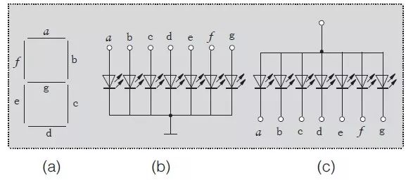

 (Pin10) and
  (Pin13). In Figure 2
  Directly connected to high level, using software to implement register clearing;
  Directly connected to the low level, the output is always valid. Connect the remaining three lines to the I/O port of the microcontroller to control the 74HC595. Data is sent to the 74HC595 from the SDI port. On the rising edge of each SCK, the data on the SDI port is shifted into the register. On the 9th rising edge of SCK, the data begins to shift out of SDO. If the first 74HC595 SDO is connected to the second 74HC595 SDI, the data is shifted into the second 74HC595. After all the data has been sent, a rising edge is given to RCK and the data in the register is placed in the latch. at this time
  When it is low, data is output from parallel ports Q0 to Q7.