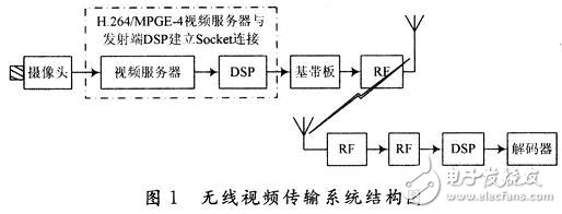
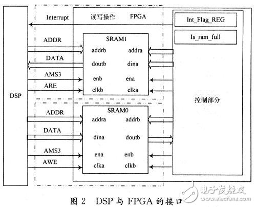
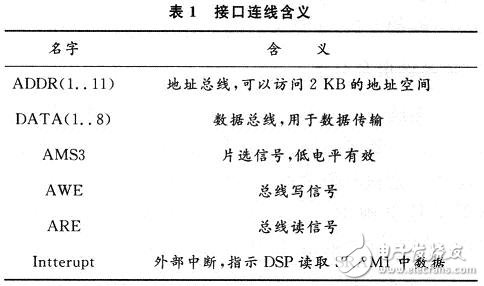
The rapid development of wireless communication technology and video compression technology has made wireless video transmission a hot topic. Wireless video transmission has the characteristics of large amount of data, high real-time requirements, and limited wireless channel resources. A new generation of video compression standard H. 264 combined with dedicated video DSF chip can meet the requirements of source coding. FPGAs that process large amounts of data, are fast, and have a relatively simple computational structure are suitable for channel coding. Based on the above considerations, a wireless video transmission system was designed, and the FPGA and data communication were configured with the transmitter ADSP-BF537 as the controller. The implementation of the system hardware is as follows: The transmitting end is composed of a camera, a dedicated video encoding chip, a control module, a baseband module, and a radio frequency module (RF). The receiving end is composed of a radio frequency receiving module, a control module, a base station module, and a dedicated video decoding chip. The system structure is shown in Figure 1. The video encoding part uses H. based on DM642. 264 video encoder. The chip transmits data through the network port, and the output video stream is H. In the 264 format, the resolution range of the output image is 176 & TImes; 144 to 702 & TImes; 576, and the code stream and frame rate can be modified according to specific needs. The control module uses Analog Devices' ADSP-BF537 as the main chip. Its main role is to complete the FPGA configuration, interface control, communication link establishment (video stream data transmission). The baseband module uses the FPGA of Xilinx Spartan3's 4 million-gate chip as the main chip. The FPGA performs the entire baseband signal processing, including channel coding, OFDM modulation, filtering, and the like. The RF module consists of four parts: the transmitting unit, the receiving unit, the frequency synthesizing unit and the external 15 W power amplifier. The differential I and Q signals are modulated, demodulated and transmitted in both directions. The transmitting unit modulates the I, Q differential input into a 340 MHz RF signal by a modulation chip, and sends it to the circulator and antenna through power control, power amplifier, and isolator; and performs transmission and reception switching through transmission and reception level control; The signal is filtered, the low noise amplifier is sent back to I, and the Q demodulation chip demodulates the differential I and Q signals, and performs RSSI detection and AGC control. The working mode adopts a half-duplex mode; the frequency synthesizing unit provides a 340 MHz local oscillator signal for the transmitting unit and a 680 MHz local oscillator signal for the receiving unit. Since the FPGA is based on the SRAM process, data is lost after power-on. In general, in addition to the boundary scan mode JTAG download, the FPGA uses more static configuration of the PROM chip corresponding to the FPGA. This configuration mode is generally not used because of the small capacity, high price, and easy burnout of the PROM. A preferred method is to dynamically configure the FPGA using a controller, such as a microcontroller or DSP. At the same time, the video server sends the video data through the network port, and needs a control part to forward the data of the video server to the forward network port, and then configures the FPGA to send the video data. Based on the above considerations, the control part of the whole system is completed by ADI's Blackfin series DSP BF537, and the DSPBF537 communicates with the video server and FPGA through the interface. 2.1 Hardware platform ADSP is a series of high-performance low-power DSP chips from Analog Devices Inc., and the ADSP-BF537 based on Blackfin processor has rich interface, excellent performance and low price, and has powerful multimedia data processing. ability. The Blackfin processor integrates a 16/32-bit embedded processor based on MSA (Micro Signal Architecture) jointly developed by Analog Devices and Intel. It supports a 32-bit RISC instruction set with a 10-stage pipeline and integrates two 16-bit units. Multiplying accelerator, the core frequency can reach up to 600 MHz. The ADSF-BF537 bus has a high-speed autonomous data channel centered on the DMA controller. The DMA bus can transfer data quickly between memories, between memory and external interfaces, and can operate in parallel with the core. ADSP's integrated development environment Visual DSP++ embeds the real-time operating system kernel VDK, suitable for multi-tasking and multi-threaded embedded operations. ADI also offers a lightweight TCP/IP (LwIP) stack port for the Blackfin family of embedded processors that can quickly network a standalone embedded application. 2.2 Hardware System Architecture DSP and video server use lightweight TCP/IP (LwIP) to exchange data, but I will not introduce it here. Mainly introduce DSP and FPGA connection. Since the FPGA is based on the SRAM process, data is lost after power down. The method adopted is to store the communication baseband algorithm file acting on the FPGA in the FLASH of the DSP. In general debugging, both DSP and FPGA need to download the program from the PC through the JTAG port. However, when the system program has been debugged, when it is necessary to go outdoors for testing or as a product, for the convenience of system debugging, the DSP self-starting and configuring the FPGA part is adopted. There are seven startup methods for ADI's ADSP-BF537 after power-on. The DSP power-on used in this design is started from 16-bit FLASH, and the startup program uses the program provided by Analog to start the FLASH program. When powering up for the first time, use JTAG, combined with ADSP's own tool "FLASH Programmer" to burn the written DSP program into FLASH. And the FPGA configuration file (.bit format) is read into the cache, programmed into the Bank1 and Bank2 of the FLASH through the DSP, and the Bank0 is used as the DSP self-start. After the power-off reset, the startup process is as follows: (1) BF537 boots from FLASH and completes DSP board level initialization. (2) The FPGA configuration file is dynamically loaded into the FPGA. (3) Using the DSP's GPIO port to perform analog timing on the FPGA's clock and data configuration dedicated pins, that is, complete dynamic configuration of the FPGA. After the startup process is completed, the DSP performs a Sock-et connection with the video server, receives the compressed video stream, and sends it to the FPGA for processing in the baseband portion. The interface between DSP and FPGA is shown in Figure 2. In Figure 2, the DSP is connected to the FPGA through its own external bus. The FPGA internally implements two 2 KB asynchronous memories SRAM0 and SRAM1. The access to the memory satisfies the timing requirements of the DSP external bus. The meaning of the interface connection in Figure 2 is shown in Table 1. For the DSP, the DSP is connected to SRAM0 and SRAM1 via an external bus, which is equivalent to the expansion of two external RAMs, which the DSP can access freely. SRAM0 and SRAM1 in Fig. 2 are used for the DSP to transmit data and receive data, respectively. SRAM0 and SRAM1 are dual-port RAMs that can be accessed by DSPs and FPGAs. This is the way to share data through this shared memory. 2.3 Software System Structure The related program was developed using Visual DSP, a DSP software development tool containing VDK (Visual DSP Kernel). VDK is a real-time operating system kernel with API function library. It has task scheduling and task management functions, and supports a total of 32 tasks. The VDK is the foundation of the entire software, and all other programs run on the Kernel. The program flow chart is shown in Figure 3. After power-on or reset, the VDK startup thread lwip_sysboot_threadtype starts running after the DSP starts. Board-level initialization and Lwip protocol stack and network port initialization are performed in the thread lwip_sysboot_threadtype, where board-level initialization includes FPGA initialization, EBIU initialization, MDMA initialization, and FLAG initialization. Next create the following threads: (1) Data transmission: video data transmission. Used to obtain the encoded video data stream from the encoder and store it in a buffer. (2) FPGA interrupt: video data transmission interrupt; MDMA interrupt. The DSP first connects to the video server through the Socket, obtains the video data from the video server, and buffers the data according to a specific format, waiting for the FPGA to trigger the video data transmission interruption. After the interrupt is triggered, the DSP starts MDMA to send a frame size of data to the FPGA transmit buffer. When the MDMA operation is completed, the MDMA interrupt is triggered and the header is written to the first two bytes of the FPGA transmit buffer. The FPGA processes the received data to the baseband algorithm and then sends the data to the RF section. After that, the FPGA triggers the video data transmission interrupt, telling the DSP that the next frame can be sent, and then starts the MDMA again. The bit error rate of the system transmitted in different SNR environments was tested. The test method is as follows: the output port of the transmitter is connected to the logic analyzer through the data cable, and the logic analyzer sends the collected frame to the PC and adds noise to the Matlab software to obtain a fixed signal-to-noise ratio. signal. This signal is transmitted to the input port of the receiving end in an uninterrupted loop. The receiver receives the signal for demodulation and transmits the demodulated data to the PC to count the bit error rate. The test results are shown in Table 2. A scheme of wireless video transmission system is designed, and the data communication process of the transmitting part is elaborated. The transfer process of data between video server, DSP and FP-GA is illustrated from two aspects: hardware architecture and software design. Among them, ADSP-BF537 is used as a controller to successfully complete the function of dynamically configuring the FPGA and transmitting video data through the network port. The solution satisfies the requirements of large data volume, real-time data processing and flexible structure, modular design. At the same time, DSP+FPGA digital hardware system development cycle is short, the system is easy to maintain and expand, suitable for real-time signal processing, so that the program has a wider range of applications.
ZGAR AZ Ice Box Vape
ZGAR electronic cigarette uses high-tech R&D, food grade disposable pod device and high-quality raw material. All package designs are Original IP. Our designer team is from Hong Kong. We have very high requirements for product quality, flavors taste and packaging design. The E-liquid is imported, materials are food grade, and assembly plant is medical-grade dust-free workshops.
Our products include disposable e-cigarettes, rechargeable e-cigarettes, rechargreable disposable vape pen, and various of flavors of cigarette cartridges. From 600puffs to 5000puffs, ZGAR bar Disposable offer high-tech R&D, E-cigarette improves battery capacity, We offer various of flavors and support customization. And printing designs can be customized. We have our own professional team and competitive quotations for any OEM or ODM works.
We supply OEM rechargeable disposable vape pen,OEM disposable electronic cigarette,ODM disposable vape pen,ODM disposable electronic cigarette,OEM/ODM vape pen e-cigarette,OEM/ODM atomizer device.
Disposable E-cigarette, ODM disposable electronic cigarette, ZGAR AZ ice box vape , Device E-cig, OEM disposable electronic cigarette ZGAR INTERNATIONAL(HK)CO., LIMITED , https://www.szvape-pen.com


