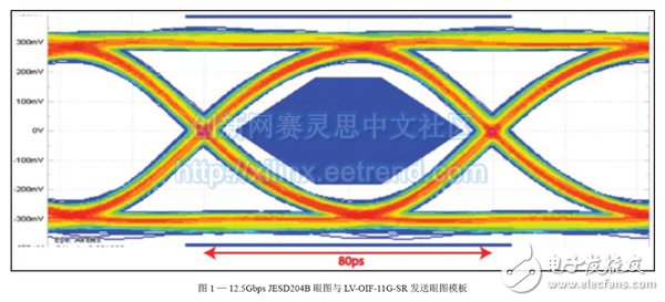
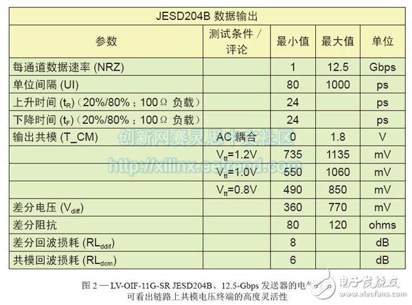
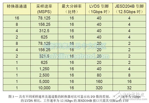
Converters built to the latest JESD204B standard are ideal for new high-speed FPGAs. I/O considerations should be considered when designing with these devices. As data converter architectures and FPGAs continue to adopt more advanced and smaller geometries, system designers face new data interface challenges. Smaller process geometries enable higher bandwidth converters to operate at ever-increasing resolutions and speeds, enabling higher data throughput. Moreover, they provide a higher serial/deserial (serial deserializer) rate to accommodate the bandwidth footprint that was not possible with previous larger geometries. Smaller process geometries also enable the integration of more data converters into a single device. These data converter interface solutions not only need to support high data rates, but must also be compatible with complex FPGA devices and guarantee I/O count. The JESD204B interface is a serial deserializer link specification that allows for maximum data rate transfers of 12.5 Gbps. This maximum data rate is supported by a converter using an advanced process (eg, 65 nm or less), which also improves power efficiency. System designers can take advantage of the technology's advantages over low voltage differential signaling (LVDS) DDR. Several open market FPGAs offer 12.5Gbps or higher data rates for serial transceivers, including the Xilinx Virtex®-7 and Kintex®-7 series. Although FPGAs have had this capability for a while, converters can now achieve this performance. This technology allows synchronization of multiple converters, such as multiple channel synchronizations within a common converter, and can be implemented in a single FPGA device. Different options for different applications For high-speed serial transmission of data converters, different applications have different options. For more than a decade, data converter manufacturers have chosen LVDS as their primary differential signaling technology. Although some LVDS applications can use higher data rates, the maximum LVDS data rate currently available to converter vendors in the market is still 0.8 to 1 Gbps. LVDS technology has been difficult to meet the converter's bandwidth requirements. LVDS is controlled by the TIA/EIA 644A specification, an industry standard for LVDS core manufacturers. This specification serves as a best practice guide for designers to improve LVDS transmitter and receiver compatibility from different vendors. Similarly, products built by designers who do not fully comply with the LVDS specification will not meet specifications and will face greater challenges in the market due to compatibility issues. Like LVDS, JESD204B belongs to the Jedec standards organization, which provides electrical and physical requirements guidance for interoperability between different manufacturers. The JESD204B's maximum data rate is defined as 12.5 Gbps, which provides an advantage over the actual LVDS throughput by more than 10 times. This performance not only reduces I/O requirements and package size for data converter systems, but also significantly saves system cost by reducing static power. The JESD204B specification supports AC coupling and is compatible with different technology nodes using different power supply stages. For example, 28nm and smaller FPGA processing nodes are typical leading edge manufacturing process technologies. Converter transistor nodes generally lag behind the industry's best FPGA generations due to the need for custom analog designs. In contrast, LVDS typically employs a DC coupling strategy that increases the difficulty of connecting the converter to a lower power power FPGA. The greater the mismatch of the common mode voltage, the higher the quiescent current consumption and will not be affected by the data rate. To this end, the JESD204B is now a fascinating differential signaling technology for high-resolution and high-speed data converter manufacturers. In addition to electrical specifications, JESD204B also has associated eye diagram performance requirements for the three physical layers. Performance metrics include defined eye diagrams and overall jitter budgets. The Optical Internet Forum (OIF) has a mature physical layer (PHY) specification and an eye diagram standard that the JESD204B interface can use to achieve the same serial data rate. The JESD204B link can use the maximum jitter allowed by the OIF Low Voltage 11 Gbit Short Range Specification (LV-OIF-11G-SR), which is 30% of the unit interval (UI). Figure 1 is a diagram of the original JESD204B eye diagram and template at 12.5 Gbps. The template provides a defined total amount of margin on the horizontal and vertical axes. It is worth noting that the 12.5 Gbps eye diagram is compliant with the LV-OIF-11G-SR specification, which is based on a speed of 11.1 Gbps and is more stringent than other 12.5 Gbps data rates. Three PHY modes The maximum and minimum electrical specifications for each category are slightly different to accommodate the necessary differences due to the wide range of data rates supported. Figure 2 shows the electrical specification parameters for the LV-OIF-11G-SR physical layer variable, which can be used for a maximum JESD204B data rate of 12.5 Gbps. One advantage of this specification is that it supports a wider common-mode voltage on the link than the DC-coupled use case. This reduces the system design requirements for JESD204B transmitters and receivers (which may come from different vendors) because it provides level shifting as needed. A second advantage of the AC-coupled data path is that it can decouple common-mode noise between the transmitter and receiver, helping to alleviate system designers' concerns about signal quality. DC coupling is more susceptible to common mode noise coupled in the data line. A third advantage of AC coupling is that it reduces the final voltage requirements of different transmitters (Vtt) and receivers from multiple vendors, allowing the receiver to operate at its optimum common-mode voltage. This helps the JESD204B transmitter and receiver operate at different final voltages in system designs that require a high degree of supply voltage flexibility. In addition, the JESD204B interface can also partition data for multiple converters on a single link. As the link rate increases to 12.5 Gbps, more converters can be deployed on the same link (corresponding to data for different variables, see Figure 3). This is especially suitable for devices that offer 2, 4, 8 and 16 converters in a single package, and this is a unique advantage over LVDS interfaces. LVDS can be used as an I/O structure to directly input and output a single-channel converter as an end point/start point, but it is not possible to explicitly define a method to integrate data from multiple converters in the entire I/O. With JESD204B, there is a clear specification for serially transmitting aggregated data from multiple converters on the same pin. The source of each piece of device data does not even need to be a real fixed hardware converter. It can come from a "virtual converter" filter that is part of the digital processing of the real converter, and the output is split into two, including real and complex paths. The IQ communication system for 90 degree phase shift can fully utilize the characteristics of the virtual converter. The explicit specification provided by JESD204B supports the simultaneous transmission of multiple converter synthesis data from the same pin. The optimal converter for the system The bandwidth requirements of higher speed converters are driving the design toward higher CMOS process nodes to reduce power consumption and improve performance. This trend will bring new interface challenges to it. The 12.5 Gbps maximum speed JESD204B interface helps solve some of these problems, otherwise even more LVDS DDR channels are needed to meet the bandwidth speed and performance requirements at higher sampling rates. Pin I/O, coupling, and power range requirements for the converter's digital interface will help you choose the right converter for your system. This 10 -port USB 3.0 hub design uses 10 USB 3.0 port to extend to your computer, laptop, reader, network camera, moving HDD, Oculus, Oculus, printers and more USB devices. 10 Port Type-C HUB 3.0, USB HUB 3.0 10 Port, 10-Port USB Hub 3.0 shenzhen ns-idae technology co.,ltd , https://www.best-charger.com
The JESD204B supports three PHY modes for serial data transmission, which are defined by the LV-OIF specification and are classified according to the maximum JESD204B channel rate. The three physical layers are defined at 3.125 Gbps, 6.375 Gbps, and 12.5 Gbps, as follows:
. Operation based on LV-OIF-SxI5: 312.5 Mbps to 3.125 Gbps;
Operation based on LV-OIF-6G-SR: 312.5 Mbps to 6.375 Gbps;
Operation based on LV-OIF-11G-SR: 312.5 Mbps to 12.5 Gbps. 

This USB 3.0 fast data transmission driver The USB 3.0 center synchronization data transmission speed is as high as 5Gbps. Compatible with Windows XP / Vista / Win 7 / Win 8 / Win 10, Mac OS 10, Linux and above, compatible with USB 2.0 Connections.