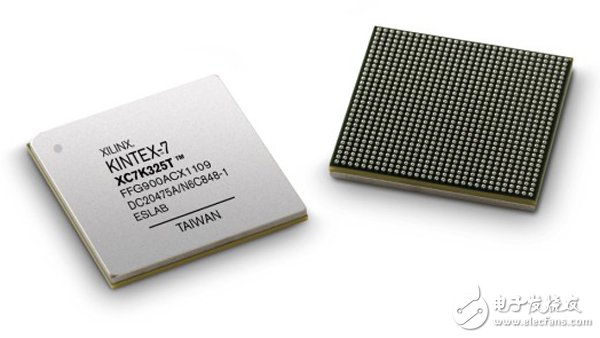
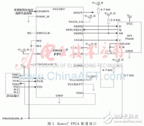
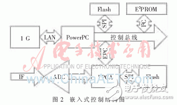
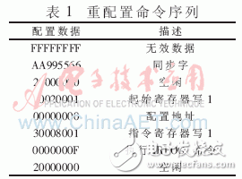
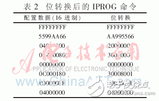
Abstract: Xilinx 7 series FPGA is the latest chip series from Xilinx. Kintex7 is one of the series of chips, with a large number of programmable resources. Even so, in some multi-mode large and complex system designs, the chip's resources are far from meeting the design requirements. Multiple loading of FPGAs can solve the problem of insufficient programmable resources. FPGA multi-loading is to store the bit files of multiple modes of design into Flash. Users can choose to load bit files of different modes according to their needs. The multiple loading of FPGA solves the problem of insufficient programmable resources and improves the utilization of FPGA programmable resources. With the rapid development of communication technology, multi-mode communication systems are widely used in modern communication, such as time division multiple access, space division multiple access, space division multiple access, frequency division multiple access and so on. The modulation and demodulation technologies are further divided into various modulation and demodulation technologies such as FM, FSK, BPSK, and QPSK. A variety of communication modes are often used in a communication system, which puts higher requirements on hardware device resources, especially the requirements of programmable chip resources. In addition, the complexity of multi-mode system design is greatly improved, and the maintenance and upgrade of the system is challenged. In recent years, FPGA technology has developed rapidly, and it is widely used as a programmable resource in the design of large-scale complex communication systems. Although FPGAs have achieved considerable results in terms of resource integration in recent years, in multi-mode large-scale system design, single-chip FPGA resources are far from meeting design requirements, and sometimes multiple chips may be required. However, FPGAs are relatively expensive, which greatly increases design costs and is not easy to upgrade and maintain. FPGA multi-loading technology [1-2] is actually the reuse of programmable resources, users can choose to load different bit files according to the needs, thus achieving multi-mode functions. FPGA multi-loading technology can solve the problem of insufficient programmable resources, improve the utilization of programmable resources, reduce the complexity of system design, increase the flexibility of system design, and reduce the coupling of multi-mode systems. System upgrade and maintenance. The hardware design of the physical connection between Kintex7 and SPI Flash is shown in Figure 1. The capacity selection of SPI Flash is related to the number of designed loading modes and the type of FPGA chip. This design implements 4 modes of switching. SPI Flash stores 4 bit files, and the capacity of SPI Flash is 512 Mbit. The control part is designed based on the PowerPC[3] processor and is used to control the entire data acquisition system. Here, only the FPGA mode load control is briefly explained. The loading mode control information of the FPGA is sent by the host computer, and the 1 G (TCP protocol) network of the host computer sends the loading mode control information to the 1 G network of the data acquisition system; the data acquisition system control part parses the TCP data packet, and extracts valid information. The loading mode is judged, and the loading information is written into the register of the FPGA through the EPC (Peripheral Controller), and the Kintex7 selects the loading mode according to the value in the register. The Peripheral Controller (EPC) is the bridge between the FPGA and the PowerPC. It is responsible for transferring the load mode information to the FPGA registers during the reload control process. In addition, the mode information after successful loading is read back and passed. The 1 G network is sent to the host computer interface to determine whether the reload is successful. The design of the embedded control part is shown in Figure 2. The IRPOG command sequence is an important part of implementing FPGA reloading. The effect of the IPROG command is similar to the effect of generating a pulse on the PROGRAM_B pin, but the IPROG command does not reset the reconfiguration [4] logic. The Kintex7 internal ICAPE2 module is capable of executing the IPROG command. The IPROG command triggers the FPGA to reload the bit file from the SPI Flash. The load address is the address specified by the WBSTAR register in Kintex7. After the IPROG command is sent, the FPGA completes three actions: sending the sync byte (AA995566); writing the next load address to the WBSTAR register of Kintex7 (table 1 address is 00000000); sending the IPORG command (0000000F). Table 1 shows the bit stream of the IPROG command sent to the reconfiguration module via ICAPE2. The MulTIboot[5] controller sends the IPROG command sequence in Table 1 to ICAPE2 using a state machine. In general, the reconfiguration controller waits for an external excitation signal. When the excitation signal arrives, the controller sends the command sequence of Table 1 to ICAPE2. Before sending the command sequence, the controller first sets the WRITE port to the low level. The rising edge of the clock sets the CE port low and then sends the sequence of instructions in Table 1. After the reconfiguration logic in the FPGA receives the IPROG command, the FPGA performs a reset operation but does not reset the reconfiguration logic and pulls the INIT_B and DONE pins low. After the FPGA clears all configuration storage, the INIT_B port is pulled high. Finally, the value of the WBSTAR register is used to reconfigure the FPGA. The IPROG command sequence is implemented by the state machine. There are at least 8 states in the state machine to generate the entire IPROG command sequence. Otherwise, the IPROG command sequence cannot be generated and the FPGA cannot be reconfigured. In addition, the transmission of the IPROG command is performed by the ICAPE2 module. The output timing of the ICAPE2 module is consistent with the output timing of the SelectMAP. The output data format of the SelectMAP is a bit conversion format, so the configuration data needs to be bit-converted during the generation of the IPROG command sequence. . Here, the bit conversion refers to the bit conversion within the byte, that is, the most significant bit becomes the least significant bit, and the bit swapping within the byte is performed as a rule. The bit conversion result is shown in Table 2. Breeze Pro Vape 2000Puffs,Breeze Pro Flavors Disposbale Vape,Breeze Pro 2000 Device Disposable,Breeze Vape Device Pro 2000 Shenzhen Zpal Technology Co.,Ltd , https://www.zpal-vape.com