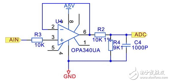
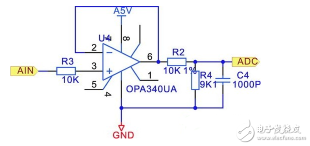
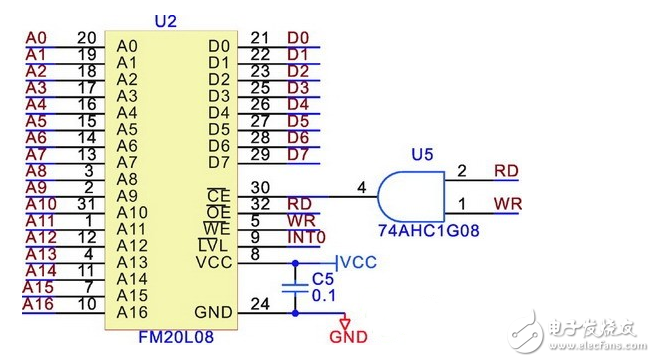
The depth of the ocean is an important parameter of ocean waters. Knowing the depth of the ocean, it can prevent ships sailing on the surface from stranding and hitting the rocks. When the submarine is operating on the seabed, measuring the depth of the ocean can use the seabed terrain as a barrier to avoid being searched, so that the other party's signal receiving instrument can not receive the noise from the submarine. In one of the subjects I did, the helicopter threw the measuring instrument from the air to the surface of the sea. After the instrument sank from the sea surface to the bottom of the sea, it automatically floated up to the surface of the sea. The project required the development of a seawater depth recorder to record the depth variation of the measuring instrument in seawater during the above process. After the measuring instrument automatically floats up to the surface, the measurement data is salvaged and played back. Depth data requires 100 samples per second and is non-volatile. The measurement data is played back to the PC through the serial port. System hardware design According to the system design requirements, the depth data acquisition frequency of seawater requires at least 100 Hz, and the continuous acquisition time is more than 5 minutes. Calculated with a 12-bit resolution ADC, the amount of data collected at a time is at least 2 & TImes; 100 & TImes; 5 & TImes; 60 = 60000B. In view of the large amount of system data collection, fast speed and strong explosiveness, the following overall design scheme is adopted: the main controller adopts the high-performance microcontroller C8051F020. It has a CIP-51 microcontroller core that is fully compatible with the 8051. It uses a high-speed pipeline architecture (25MIPS). Most of the instruction execution time is 1~2 clock cycles. It has 64KB of system-programmable FLASH and large-capacity internal SRAM with external Memory interface. The non-volatile memory uses the FM20L08 ferroelectric memory of Ramtron Corporation of the United States. Compared with other types of non-volatile memory, FRAM ferroelectric memory has the characteristics of high read and write times, fast read/write speed, low power consumption, no delay and no erase write operation, and can completely replace SRAM in function. . The system hardware block diagram is shown in Figure 1. Figure 1 system hardware block diagram Signal conditioning circuit design The signal debugging circuit is shown in Figure 2. Figure 2 signal conditioning circuit Although the C8051F020 has a 2.43V reference internally. However, the test results show that the output voltage fluctuates greatly with temperature, which affects the accuracy of the measurement results. In order to improve the measurement accuracy, the system uses Maxim's low temperature drift voltage reference chip MAX6325. The MAX6325 is a low temperature coefficient (1ppm/°C), low noise (1.5mVp-p) voltage reference with an initial accuracy of ±0.02%. It is ideal for high precision data acquisition systems. Since the output voltage range of the pressure sensor is DC1~5V, the voltage reference of the MAX6325 output is 2.50V. It is therefore necessary to attenuate the pressure sensor output voltage to match the reference voltage. The easiest way to achieve this is to divide the voltage directly with two resistors, but since the sensor has a certain output impedance, directly matching the divider resistor is equivalent to connecting the sensor output impedance in parallel with the two resistors, which will cause the input A/D. The sampling voltage is not accurate. The correct method is to add an operational amplifier to increase the input impedance after the output of the pressure sensor, and then connect the voltage divider resistor in the output stage of the op amp. Considering that the system only has 5V voltage and the output voltage of the sensor is between 1~5V, and also to reduce the number of devices and reduce the board area, the op amp selects OPA340. The OPA340 is a single supply rail-to-rail input and output operational amplifier. The OPA340 operates down to 2.5V, allowing a minimum input of -500mV and a maximum input of 500mV above the power supply. Data storage circuit design For recorders, high-speed storage test equipment, etc. for burst data, the high-speed storage and power-down of data is not lost, the Ram20 company's FM20L08 ferroelectric memory makes up for the small amount of existing ferroelectric memory. Disadvantages, its data storage capacity of 1Mb (128KB), can completely replace the standard asynchronous static random access memory (SRAM), with the ability to randomly read and write any byte in the chip. The FM20L08 non-volatile ferroelectric memory can read and write indefinitely. After power-off, the data can be stored for 10 years and the working voltage is 3.3V. The maximum power consumption is 22mA and is available in a 32-pin TSOP package. The FM20L08 adds software-controlled write protection. The memory sequence is arranged in 8 areas by address. Each area can be individually written and protected by software. In the real-time acquisition and recording of seawater depth, in order to better understand the process of instrument depth variation in water, high-speed data acquisition and a large amount of data storage must be guaranteed. The high-speed writing and power-down data loss characteristics of the ferroelectric memory are perfectly suitable for such situations, and the complete process of the falling of the object in seawater can be completely recorded. Figure 3 shows the interface circuit of the C8051F020 and FM20L08. Figure 3 interface circuit of FM20L08 and C8051F020 The C8051F020 uses the upper port (P4~P7) to interface with the FM20L08. The FM20L08 adds an internal voltage monitor to drive the LVL (LowVoltageLockout) signal, which is connected to the INT0 of the MCU to monitor the power supply of the power supply. When the power supply voltage drops below the critical value, the LVL pin outputs a low voltage signal, and the display circuit is in The write protection state resets the MCU in the MCU's INT0 interrupt service routine, so that the memory can automatically prevent false reads and writes and prevent the destruction of stored page data. The chip select signal of FM20L08 is controlled by the C8051F020 read/write signal phase. As long as any of the read/write signals goes low, the chip select signal is valid. The C8051F020 has a maximum address space of 64K, and requires it to access 128KB of address space. The easiest and most efficient way is to use an I/O bit to control the address line A16 of the FM20L08. When A16 is 0, the first half of FRAM is selected. When A16 is 1, the second half of FRAM is selected. In the storage program design, the program should first determine whether the input signal value of the A/D is greater than the threshold when the instrument is falling. Only when the input signal value is greater than the threshold value, the data is stored in the storage unit, and the measuring instrument is floated from the sea bottom. Turn off the ferroelectric memory when it is about to approach the sea and stop data storage. Wireless Charging Multifunctional Sterilizer Phone Sterilizer,Mobile Phone Sterilizer Box,Wireless Charging Uv Sterilizer Box,Wireless Charging Multifunctional Sterilizer wzc , https://www.dg-wzc.com

