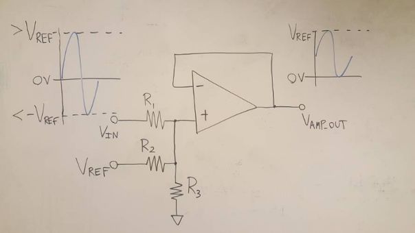
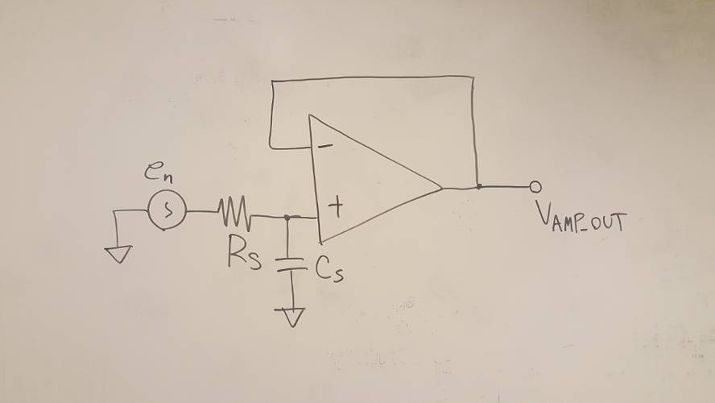
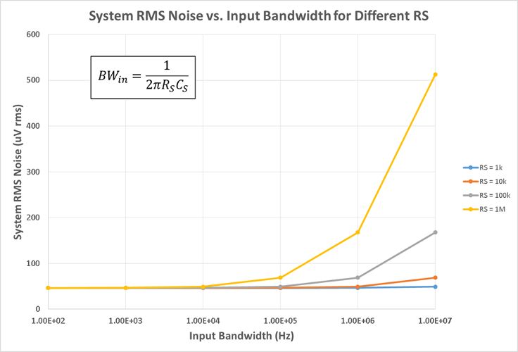
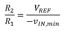
How to use the ADAQ798x series of μModule data acquisition system with all-in-one ADC that combines flexibility and high integration? ADI engineers have written six blogs to help you get the most out of the flexible front end of the ADAQ798x family and explain how it can be configured to suit different applications. Before we shared the first two articles of the series, we mainly introduced two issues. How do I interface with a unipolar input source that is smaller than the ADC input range? Why configure an ADC driver? Click to view → Almighty ADC, you should use it (on serial) to view it. Today, let's take a look at the third and fourth chapters of this series of blogs - in- phase summing configuration and in- phase summing configuration that supports attenuation. The bipolar signal swings up and down at a low voltage (0 V). Since the ADAQ798x integrated ADC can only convert 0 V to V REF signals, the bipolar signal needs to be DC biased and properly adjusted for this ADC. To accomplish this, the following configuration adds two resistors (R 1 and R 2 ) to the standard in-phase configuration . This configuration sums the input signal to a separate DC voltage to bias the ADC driver output to the ADC midscale input (V REF /2) for bipolar to unipolar conversion. It is often feasible to use the reference voltage (V REF ) as a DC voltage so that no other circuitry is needed (the ADAQ798x is always accompanied by a reference!). It also prevents V REF bias from adding offset errors to the system because the DC bias of the ADC driver is always half of V REF . For these reasons, we will specifically discuss this configuration that uses V REF as the DC "transform" voltage. The transfer function for this configuration is as follows: Similar to the normal in-phase configuration, the ratio of Rf to Rg determines the gain from IN+ to AMP_OUT, but this ratio now also depends on the input amplitude of the vIN. Note that vIN is bipolar, but the voltage on the in-phase node is unipolar. This means that the voltage on IN+ must be 0 V corresponding to the minimum value of vIN: This relationship gives the ratio of R1 to R2: Rf and Rg can be determined using the transfer function of this configuration and the condition that the ADC driver output (vAMP_OUT) is equal to VREF/2 when vIN is 0 V. Solving the equations for Rf and Rg gives: Now there is the ratio of R 1 to R 2 and the ratio of R f to R g , but we also need to pick a specific value. We have discussed the choice of R f and R g values in the series "Adding Gain for Unipolar Inputs" . The choice of R 1 and R 2 should be based on the applied noise, accuracy, and input impedance requirements. A small resistor improves noise and reduces the offset error caused by its interaction with the ADC driver input bias current. However, to increase the input impedance and reduce the output current of the reference source, a large resistor is required. The input impedance of this circuit is: Note that for the special case where the vIN amplitude is ±VREF, the ratio of Rf to Rg is zero. In this case, the ADC driver gain is 1, meaning that Rg is omitted and Rf can be 0 Ω. The ADAQ7980 requires a bipolar to unipolar conversion of the ±1 V input signal, V REF = 5 V, using R f = 2 kΩ. Using the above formula, R 2 must be 5 times R 1 and R f must be 2 times R g . R f is 2 kΩ, so R g must be 1 kΩ. The specific values ​​of R 1 and R 2 can be selected according to the application requirements. For this example, we want to choose a combination of R 1 and R 2 to offset the effect of the input bias current on the offset error. As stated in the technical article "Operational Amplifier Input Bias Current" , for this purpose, R 1 ||R 2 should be equal to R f ||R g , so R 1 = 800 Ω and R 2 = 4 kΩ. Let us consider another example: vIN = ±10 V, VREF = 5 V. In this case, we will encounter the problem that the ratio of Rf to Rg is negative, so this input range cannot actually be realized with this configuration. In fact, the maximum vIN for this configuration is ±VREF, at which point the ADC driver gain is equal to one. Fortunately, we'll discuss the other two configurations that allow us to go beyond this input range in the next article in this series. The above configuration can also be used for unipolar signals if R2 is grounded instead of VREF. This modification is useful for unipolar input signals (amplitude greater than VREF) that require attenuation for the ADC. In this case, the ADC driver is most likely to be unity, so Rf and Rg are not required. As mentioned above, if the application requires high input impedance, then R1 and R2 must be large, which may increase the noise floor of the system. We can compensate for the noise increase by increasing the shunt capacitance and/or by oversampling and decimation. Both schemes reduce the noise floor by losing the input signal bandwidth. However, for low bandwidth or DC applications, the input bandwidth is less important. Therefore, these configurations are better suited for low bandwidth, high input impedance applications. We will discuss this topic in more detail in the next article. However, one problem that is not addressed is the offset error caused by the input bias current of the ADC driver flowing through the resistor. The larger the resistance, the greater the DC error caused. This error can be reduced by adjusting the ratio of R1 and R2 to compensate for unwanted voltage drops, or by offsetting the values ​​of Rf and Rg to offset the offset caused by R1 and R2, but the input range is lost. However, it should be noted that Rf must be small enough to ensure that the amplifier is stable, so the second option is not always feasible. For signals greater than ±V REF , the following configuration can be used to perform bipolar to unipolar conversion with attenuation. This configuration is similar to the configuration discussed in [In-phase summation configuration] above, except that Rf and Rg are no longer needed, but R3 is added to provide additional signal attenuation. The transfer function for this configuration is as follows: The mathematical calculation of the ratio of R1, R2 and R3 is complicated, but we can use a similar method to the previous configuration. After determining the ratio of the resistance, you can select a specific value according to the application requirements. For the sake of brevity, each step of the derivation is not described here, but we will see that for the minimum and maximum values ​​of vIN, the simplification of the transfer function allows us to derive the resistance ratio. The ratio of R1 to R2 is derived using the transfer function of this configuration and substituting the minimum value of vIN (so that vAMP_OUT is equal to 0 V): R3 does not appear in the formula. Solving R1 and R2 yields: The ratio of R1 to R3 is derived by substituting the maximum value of vIN (so that vAMP_OUT is equal to VREF): This time, R2 does not appear, and R1 and R3 are solved: At this point, we can choose the value of either resistor (considering the VREF and vIN ranges) and then calculate the values ​​of the other two resistors. As before, the main trade-offs are input impedance and system noise and offset errors. The input impedance (ZIN) of this circuit is: Consider again the example of the [In-phase summation configuration] section above, where vIN = ±10 V, VREF = 5 V, and the configuration is designed with an input impedance of 1 MΩ. For this combination of vIN and VREF, R1 must be twice the R2 and equal to R3. Use the ratio of R2 and R3 to R1 for the input impedance equation to get R1 = 750 kΩ. Therefore, R2 and R3 are 375 kΩ and 750 kΩ, respectively. As described in [In-phase summation configuration], the input impedance and system noise performance need to be weighed. Achieving high input impedance requires large resistors, which generate more thermal noise and interact with the input current noise of the ADC driver to generate more input voltage noise. Both increase the effective rms voltage noise at the ADC input, resulting in a significant performance degradation. In the above example, the total system noise is approximately 334 μV rms (with a 5 V reference, the dynamic range is reduced by a full 15.5 dB from 92 dB to 74.5 dB)! But there is hope! This configuration can actually achieve near optimal performance if the input bandwidth is limited. For example, if the input bandwidth in the above example is limited to 20 kHz, the overall system noise is reduced by a factor of 10 to 48 μV rms (for VREF = 5 V, the dynamic range is 91.4 dB)! We can limit the input bandwidth (BWin) by increasing the shunt capacitor CS, as shown in the figure below. Note that for these noise calculations, we can think of R1, R2, and R3 as a single resistor RS, where RS is a parallel combination of R1, R2, and R3. The Technical Guide, Operational Amplifier Total Output Noise Calculation for Single-Pole Systems, shows how to calculate the noise generated by RS (including thermal noise and its interaction with the input current of the ADC driver). The main difference between the ADAQ798x is that the noise bandwidth is set by the integrated RC filter, not the amplifier bandwidth in the guide. The rms noise added by RS to the ADC input is: (en is the Johnson noise of RS and G is the ADC driver gain.) CS reduces the noise reaching the ADC by reducing the input bandwidth of the ADC driver. If the cutoff frequency of RS and CS is much smaller than the cutoff frequency of the integrated RC filter (4.42 MHz), the noise contribution of RS can be calculated using RS and CS instead of R and C in the above equation. The total system noise is the sum square root of each noise source in the ADAQ798x, including the noise of the RS, the input voltage noise of the ADC driver, and the rms noise of the ADC. The figure below shows the relationship between system noise and input bandwidth for multiple RS values. Note that as the input bandwidth decreases, system-wide noise tends to the total rms noise of the ADAQ798x (44.4 μV rms). This means that the noise reduction gains obtained by reducing the bandwidth are decremented at a frequency that depends on the RS rms value. This section discusses an ADC driver configuration that allows the ADAQ798x to accept bipolar inputs greater than ±VREF and shows how to calculate input impedance and system noise based on the resistance value (and optional shunt capacitance CS). Although it has been shown that increasing CS reduces noise, it also limits the available input bandwidth. Therefore, when using this configuration for wide bandwidth applications, it is often impractical to achieve high input impedance. This configuration is only recommended for low bandwidth applications that require high input impedance. Fiber Optic Splice Closure,Fiber Optic Splice Case,Fiber Splice Closures,Outdoor Fiber Optic Splice Closure Cixi Dani Plastic Products Co.,Ltd , https://www.dani-fiber-optic.com In-phase summation configuration
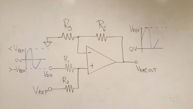




 for example
 In-phase summation configuration that supports attenuation