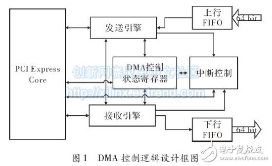
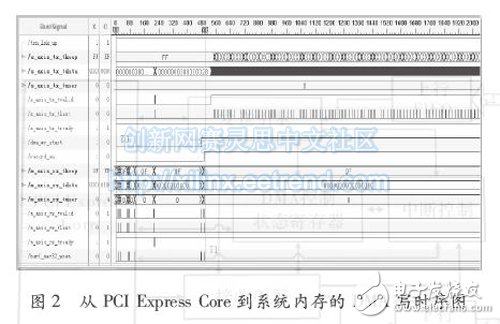
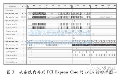
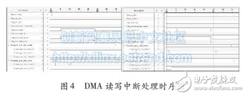
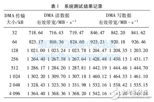
Abstract: Based on the embedded PCI Express Core in Xilinx Virtex-6 FPGA, this design implements DMA read and write initiated by PCI Express board, which can complete high-speed data transmission between PC and PCI Express board. The design has been debugged on the Xilinx evaluation board ML605. The DMA write memory speed is stable up to 1 520 MB/s, meeting the requirements of high-speed storage systems. With the advent of phased array radars, ultra-wideband radars, and digital array radars, the amount of radar echo data is constantly increasing, and therefore higher and higher requirements are imposed on high-speed acquisition and large-capacity data transmission. Early high-speed data acquisition systems based on PCI bus have certain defects in bandwidth, flow control and data transmission quality, and to some extent, they cannot fully meet the requirements of high-speed and large-capacity data storage. In comparison, the PCI Expres bus has a distinct technical advantage, not only is fully compatible with the PCI bus, but also comprehensively solves the bandwidth, flow control and data transmission quality problems faced by the PCI bus. Due to the use of a high-speed differential bus, the clock frequency can be reached. At a higher level, the bus bandwidth is also significantly improved compared to the PCI bus. At present, the X16 PCI Express peak bandwidth can reach 80 GT/s. The gradual maturity of PCI Express technology provides a better solution for high-speed data transmission. The DMA control logic design is shown in Figure 1. There are key modules such as PCI Express Core, Receive Engine, Transmit Engine, DMA Control Status Register and Interrupt Control. The main features are as follows: (1) Comply with the PCI Express Base SpecificaTIon 2.0 specification. (2) Support X1, X2, X4 or X8 mode. (3) The on-chip GTP/GTX transceiver implements the PHY. (4) A management interface with access to the PCI Express configuration space and internal configuration. (5) Support for the largest payload (128 to 4 096 Bytes). (6) A base address register (BAR) that can be configured for memory or I/O. In the PCI Express system logic structure, the receiving engine mainly analyzes the memory read and write requests according to the basic TLP receiving timing under the control of the interface clock, and extracts the required information from the TLP and transfers it to the memory access controller, and the memory accesses The controller processes the data written to the memory in the memory write TLP and uses the data read in the memory to respond to the memory read TLP; in addition, the accept engine is primarily responsible for processing the memory read completion TLP, in response to the board initiated DMA read operation. In the PCI Express system logic structure, the sending engine mainly generates the completion packet for the received memory read TLP according to the basic TLP transmission timing under the control of the interface clock, and the information required to generate the completion packet is transmitted by the storage controller. To the sending engine; in addition, the sending engine is also responsible for initiating a memory read and write request TLP to implement DMA reading and writing of data with the PC. In the PCI Express system logic structure, the DMA status control register is mainly to transfer data between the PCI Express Core and the Root Complex. The Windows GUI software configures the DMA Control Status Register to control DMA operations. The DMA Control Status Register is mapped to the PCI Express Memory BAR0 space, and the Windows GUI software accesses the registers through the Memory Write and Read cycles. The Windows GUI software initializes the DMA control register to initiate a DMA transfer, and through the status register, notifies the Root Complex that the DMA transfer is complete. When the DMA transfer ends, in order to notify the PC of the response in time and process the interrupt, the interrupt control section generates an interrupt using the configuration layer interface signal of the core. PCI Express supports two types of interrupts: Message Signal Interrupt (MSI) and Legacy INT. In the PCI Express device enumeration process, the association will set the command register and message signal interrupt capability register in the configuration space according to its own ability to interrupt support to determine which interrupt to use. Data flow: Upstream FIFO data → PCI Express Master DMA Write → PC Memory → PC Hard Disk. The entire DMA write process is as follows: (1) Reset the FPGA logic with a delay of 1 ms; remove the FPGA logic with a delay of 1 ms. (2) Detect hardware link initialization. (3) Turn on the DMA write completion interrupt. (4) Set the DMA write destination address register and set the DMA write transfer length register. (5) Start the DMA write operation and select the record path. (6) Wait for the DMA write completion interrupt. (7) Clear the interrupt and the memory data is transferred to the hard disk. (8) Whether the DMA write is finished, if yes, go to step (9); otherwise, go to step (4). (9) Terminate the DMA write, close the DMA write completion interrupt, and disconnect the record path. The DMA write timing from PCI Express Core to system memory is given below, and Figure 2 is a timing diagram taken with ChipScope. M_axis_rx_tvalid and m_axis_rx_tlast are valid 8 times together on the core receiving transaction interface between T0 and T1, that is, 8 PIO memory read and write operations are performed. The sixth time is the PIO read operation. The corresponding send transaction interface is valid for s_axis_tx_tvalid and s_axis_tx_tlast, and the Cpld completion packet is generated in response to the PIO read operation. As can be seen from the figure, after the DMA status control register is configured, the dma_wr_start signal is valid, that is, the DMA write operation is started. After that, the PCI Express Core starts to send the memory write transaction packet on the sending transaction interface. The address and size of the transaction packet have been configured in the DMA status control register. Data flow: PC hard disk → PC memory → PCI Express Master DMA Read → Downstream FIFO data. The entire DMA reading process is as follows: (1) Reset the FPGA logic with a delay of 1 ms; remove the FPGA logic with a delay of 1 ms. (2) Detect hardware link initialization. (3) Turn on the DMA read completion interrupt. (4) Set the DMA read destination address register and set the DMA read transfer length register. (5) PC hard disk data is transferred to the memory. (6) Start the DMA read operation and select the playback path. (7) Wait for the DMA read completion interrupt. (8) Clear the interrupt and the hard disk data is transferred to the memory. (9) Whether the DMA reading is finished, if yes, go to step (10); otherwise, go to step (4). (10) Terminate the DMA read, close the DMA read completion interrupt, and disconnect the playback path. The DMA read timing from system memory to PCI Express Core is given below. Figure 3 is a timing diagram taken with ChipScope. The m_axis_rx_tvalid and m_axis_rx_tlast are validated three times together on the core receiving transaction interface between T1 and T2. It should be noted here that the DMA read operation needs to transfer data from the PC hard disk to the data buffer of the memory development after configuring the register, and then the DMA read operation can be started. Therefore, the m_axis_rx_tvalid on the core receiving transaction interface between T1 and T2 is M_axis_rx_tlast is valid for configuring the DMA read address and starting a DMA read operation. After the DMA read operation is started, the s_axis_tx_tvalid and s_axis_tx_tlast are valid on the core transaction interface, and the memory read request packet is sent. When the PC receives the memory read request packet from the PCI Express Core, the PC will reply to the corresponding Cpld completion packet according to the information in the TLP. . According to the PCI Express bus specification in the PCI Express bus specification, the receiving transaction interface is allowed to transmit the memory read request packet while receiving the Cpld completion packet, as shown in the figure between T1 and T2. When the DMA write ends, that is, one of dma_wr_done or dma_rd_done is valid, the user should commit the interrupt by configuring the interface cfg_interrupt and cfg_interrupt_assert. When the core receives a valid interrupt, it sets cfg_interrupt_rdy to be valid, indicating that the interrupt request is accepted. The PC recognizes the interrupt transaction by reading the DMA interrupt register, and clears the interrupt after responding to the processing interrupt. The interrupt sequence is completed by the DMA read and write captured by ChipScope, as shown in Figure 4. The system performance test results are shown in Table 1. The memory read and write DMA data effective bandwidth test is DMA boot to the last memory write TLP or the last memory read completion packet, the total test data is 8 GB. Test platform: Xilinx ML605 development board (Virtex-6 FPGA); Windows7 64-bit operating system, Windriver driver; PCI Express link width: X8, PCI Express Core version: V2.5; MaxPayload Size: 128 Bytes; Max Read Request Size: 512 Byte; Root Complex Read CompleTIon Boundary: 64 Byte. The high-speed DMA read/write design based on Xilinx PCI Express Core is studied, which is suitable for the requirements of modern radar systems and high-speed data acquisition systems, and has good portability and scalability. The DMA design block diagram is given in this paper, and the various parts of the system are analyzed. The system design mainly studies the PCI Express Master DMA read/write design and interrupt control, and gives the sampling timing of DMA read/write and interrupt control. Through the system performance test data, we can see that the Xilinx PCI Express Core based on this design is based on this. High-speed DMA reading and writing can meet the requirements of high-speed signal processing. FTTA IP68 Hardened Connections Ftta Ip68 Hardened Connections,Ftta Ip68 Hardened Connections Adapter,Ftta Ip68 Hardened Connections Box,Ftta Ip68 Hardened Connections Cable Huizhou Fibercan Industrial Co.Ltd , https://www.fibercan-network.com