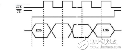
The SPI bus system is a synchronous serial peripheral interface that allows the MCU to communicate serially with various peripherals to exchange information. It is because of the way of communication that we can control a wide variety of peripheral devices through the chip to achieve a lot of "unbelievable" modern technology. Here we will introduce the SPI bus from a programming perspective with the SPI title. Figure 1 SPI interface SPI is an abbreviation for English Serial Peripheral interface, which, as its name suggests, is a serial peripheral interface. Motorola was first defined on its MC68HCXX family of processors. SPI is a high-speed, full-duplex, synchronous communication bus. Due to its easy-to-use features, many of the nor flash and nandflash chips now integrate this communication protocol, which is what we call SPI flash. Figure 2 SPI application SPI flash chip is widely used, and it has more or less traces on many electronic products, such as mobile phones, digital, liquid crystal displays, set-top boxes, computer motherboards, etc. Recently, it was revealed that Apple's new mobile phone iPhone 8 will be introduced with coded flash memory (NOR Flash), which makes the NOR chip that is already out of stock more annoyed. According to the storage industry, this year's NOR chip supply gap will be possible. Expand to 20%. The SPI interface typically uses 4 lines of communication, MISO master data input, and slave device data output. MOSI master device data output, slave device data input. The SCLK clock signal is generated by the master device. The CS slave selects the signal and is controlled by the master. Figure 3 SPI bus The SPI interface generates the slave enable signal and the clock signal under Master control, and the two bidirectional shift registers perform bit-by-bit transmission for data exchange, and the transmission data is high and the low bit is (MSB). The data changes on the falling edge of SCK, and one bit of data on the rising edge is stored in the shift register. Figure 4 enable signal and clock signal After understanding the SPI protocol, let Xiaobian take you to easily operate the SPI flash chip. The operation of the flash chip generally includes the erasing, programming and reading of the flash chip. The SPI flash chips of all major manufacturers are similar, and the operation commands are basically unchanged. When we get a chip, we must pay special attention to the chip. The capacity, operation partition, the following takes Wang Hong's chip as an example for everyone to explain. In fact, whether it is the chip erase, programming or read operation, we can roughly follow the following routine: write command --- write address --- write (read) data. As the following timing diagram is as clear and clear, we first pull the chip select signal low, then send a 0x02 page programming command, and then send an address, you can easily write data. According to the sample hoist, the erase operation is the same, even simpler, but we should pay attention to the WIP bit of the loop judgment status register until the completion of the erase, the specific cycle time depends on the chip. In addition, we must pay special attention to the OTP area of ​​SPI flash, that is, (ONE TIME PROGRAMMABLE), that is to say, this area can only be programmed once, and can not be modified and erased after programming, so we must pay special attention when operating. Before reading and writing to the OTP area, we must first send a command to enter the OTP area. The other operations are the same as those of the above normal flash area. With the above methods, we can easily operate the SPI flash chip. Of course, the underlying operation of timing requires continuous learning and accumulation.
* ★High Quality replacement AC adapter for Nintendo Wii gaming console,WII charger can customized your logo Input: 100V-240V; Output: 12V 3.7A; Cable Length: 8.3FT(2.5M); Material: Metal /+Plastic
* ★Durable power adapter equipped with auto-voltage function.WII AC adapter poer cord
* ★Kind note:This AC power cord is compatible With NINTENDO Wii only,not for WII U.
* ★100% test one by one via console before shipping
* ★UK US EU Plug are available, Made from durable material for long time use, and with auto voltage feature that allows the adapter to be used worldwide
* ★Very easy to use,Durable power adapter allows you to have maximum portability and game time, seamless plug and play charging, extended life guarantee.
Nintendo Wii Adapter,Power Supply For Nintendo Wii,Wii Ac Adapter Power Supply,Wii Power Supply Shenzhen GEME electronics Co,.Ltd , https://www.gemesz.com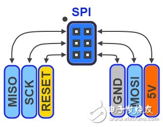



* ★Convenient spare if using your console in multiple rooms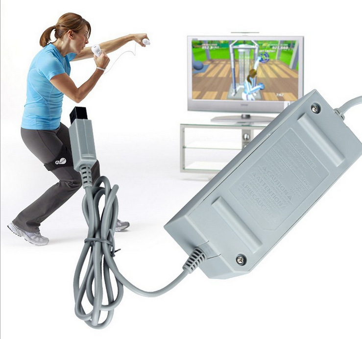
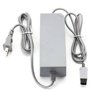
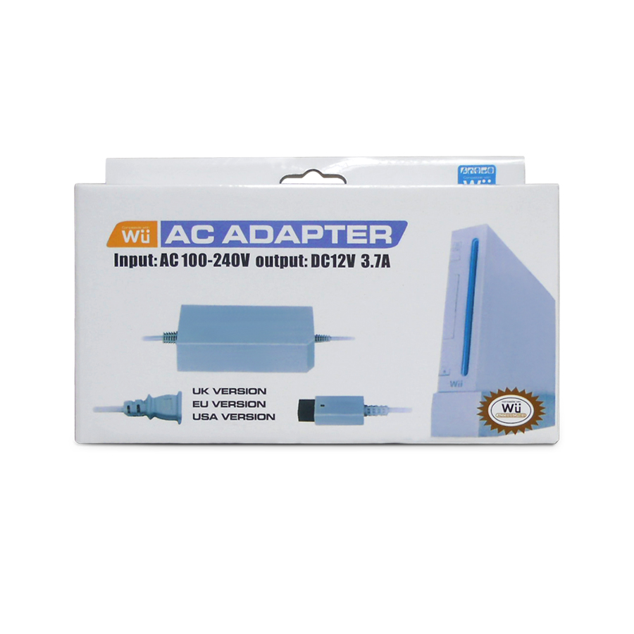
* ★Universal voltage - Input: 100V-240V; Output: 12V 3.7A; Cable Length: 7 feet
Read the SPI serial peripheral interface
Product Name
AC DC Adapter for WII Console
weight
450g with box
Input
100-240V
Output
12V- 3.7A
Product color
Gray
Product size
13x5.4x4cm/5.12x2.13x1.57 inch
Cable length
150cm + 100cm
OEM/ODM
warmly welcome
Advatage
100 QC test before shipping
Delivery Method
DHL,TNT,UPS , FEDEX ETC