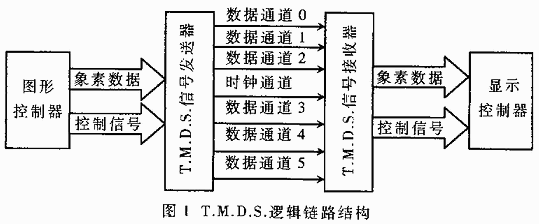
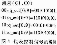
Abstract: Introduces the development background and technical advantages of the new digital video interface, and analyzes the communication protocol of DVI 1.0 and T. M. D. S. The link configuration, signal characteristics, encoding and decoding algorithms of the link are analyzed for the actual application, and the clock configuration of the DVI interface is analyzed. Finally, the related protocols such as DDC, EDID, and HPD are briefly introduced. 1 Introduction The first light of the 21st century has just emerged. When people are enjoying high-speed microprocessors that increase with Moore's Law, a new type of video interface technology will bring people a more colorful visual experience. This is the DVI? Digital Visual Interface? Digital video interface technology that the industry has just developed. With the rapid development of digital flat panel display technology represented by LCD, DVI will quickly become the standard video interface for computer display. With the advocacy of the concept of green display, CRT display has developed from spherical to cylindrical, and from cylindrical to flat display. People have higher and higher requirements for screen refresh rate and image geometric distortion. Traditional analog VGA video interface + CRT Or the image display capabilities of LCD monitors are becoming increasingly stretched. The continuous reduction in manufacturing costs has led to flat panel display technologies such as LCDs gradually replacing traditional CRT monitors and becoming the mainstream of PC monitors. Because it is compatible with the traditional VGA analog interface, it has to have a built-in ADC? Digital-to-analog converter? And PL? Phase-locked loop? Circuit to convert the analog video signal into a digital signal and then display it. The displayed value is corrected to obtain a gray signal suitable for the LCD pixel characteristics. The conversion of such a series of intermediate links, coupled with the problem of noise interference that is difficult to suppress in the analog transmission link, causes the image information displayed on such flat panels to be lost and increases with the increase in resolution and field frequency. The vigorous development of flat panel displays (including digital projectors) represented by LCD, PDP, LED, OLED, etc. has put forward urgent requirements for digital video interface technology. 2 DVI interface structure The DVI interface uses the smallest transformed differential signal—T. M. D. S. ? Transitionation Minimided Differential Signal? As the basic electrical link signal. T. M. D. S. The link is mainly used to transfer image data to the display. DVI interface protocol allows the use of dual T. M. D. S. Link structure, which can support the display device of super large resolution. T. M. D. S. The 8-bit pixel data is converted into a 10-bit minimum conversion signal through an advanced coding algorithm, which weakens the cross-electromagnetic interference EMI in the transmission cable, and this DC-balanced coded signal is more conducive to fiber transmission. In addition, this advanced coding algorithm can provide a clock recovery signal for the receiving end, and allows the signal to have a larger jitter error when transmitted over a longer distance (generally less than 5m). 2.1 DVI architecture requirements As a video interface for computer development, DVI should be compatible with the existing operating system and hardware platform, and also maintain certain compatibility with the previous interface standards. Figure 1 shows the DVI interface. M. D. S. Logical link structure. DVI supports Plug and Play (Plug and Pay). When the system starts, DVI provides the lowest resolution VGA 640 × 480 mode? The system accesses the display through the DDC2B protocol to obtain support for the pixel format of the display, and obtains information about the display model and realistic capabilities through EDID data. These contents are a piece of data solidified by the display manufacturer within the display, and provide its own information to the host system through DDC? Disply Date Chanel ?. Of course, the DVI interface also supports technologies such as hot plugging (Hot Plug Device) and display power management? There are also compatibility issues with traditional analog VGAs. These are just the compatibility problems that DVI must do as an interface standard, and do not represent the advanced nature of DVI. Refer to References 1-3 for questions about these system requirements. 2.2 T. M. D. S. Detailed agreement The advanced nature of the DVI interface is reflected in that it can transmit massive display information to the display at high speed. M. D. S. Advanced coding algorithms are the basis for its powerful capabilities. The following will explain T in detail. M. D. S. Several issues in the agreement that are closely related to the actual application. For ease of understanding, the following provisions are made: the pixel data input to the encoder or output by the decoder is called pixel data? Picture Data ?; the encoded data sent by the transmitter or input to the receiver is called a symbol? . Please note: The DVI interface protocol does not specify whether the input or output pixel data is serial or parallel. The input and output data format is left to the chip manufacturer to flexibly control. The user should choose the chip model according to his actual situation. 2.2.1 Link structure T. M. D. S. The link structure is shown in Figure 2. Figure 3 is a single link T. M. D. S. Structural drawing. The dual link structure is very similar to the single link. The transmitter of each link contains three identical encoders, each of which drives a serial T. M. D. S. Channel (Chanel). The data input to each encoder includes 8bit pixel data and 2bit control signals (see Figure 3). Under the control of DE (Data Enabling) signal, under any legal clock drive, the encoder encodes pixel data and control data separately, and the encoded symbols are serially sent by the transmitter to T. M. D. S. On the link. Pixel data is coded and sent during the DE valid period (DE = 1), and control data is encoded and sent during the DE invalid period (DE = 0). Regardless of which of the two is encoded, the encoder outputs serial 10 bit symbols, and the least significant bit is sent out first. Clock and synchronization are a vital part of the DVI signal processing. Taking the pixel clock (Pixel Clock) provided by the graphics processor in the graphics card as the reference clock, there will be three sets of clock signals with different frequencies in the entire signal transmission and reception process. These three sets of clock signals are carried out through the phase-locked loop circuit (PLL) Synchronous control. It can be seen from Figure 3 that the 8-bit pixel data input to the encoder at the speed of the pixel clock is transformed into a 10-bit T. M. D. S. Symbol, in T. M. D. S. Serial transmission in the channel. So T. M. D. S. The symbol should be transmitted at the clock frequency of 10 times the pixel. At the receiving end, if you want to correctly judge the received symbol, you need to sample the input signal at a frequency higher than the code clock? Chakrater CLOCK ?, so there is another sampling clock? Sampling Clock ?. For example: DVI receiver chip provided by TI company? 6? Use 4 times oversampling technology to sample the input signal, at XGA resolution (1024 × 768), T. M. D. S. The advanced coding algorithm makes the serial output symbol stream contain symbol synchronization information. Using the PLL technology, the receiver and decoder can correctly determine the symbol boundary and decode pixel data in the serial symbol stream. At T. M. D. S. In the output code, the code representing the pixel data contains the change information of 5 times or less, and the code representing the control signal contains the conversion information of more than 7 times. These codes containing high-variation information are sent out during the displayed blanking period. The decoder can uniquely identify these high transform codes, and the PLL can use these determined signals as reference signals for phase correction. 2.2.3 T. M. D. S. Encoding and decoding algorithms Deep understanding, flexible use and implementation of these advanced algorithms are the most concerns of chip manufacturers. This article analyzes the encoding and decoding algorithms from the user's point of view, using the principle of practicality. As can be seen from Figure 3, the line synchronization and field synchronization signals that are most concerned in practical applications are used as control information in the blue primary color? Blu? 7? 0 ?? is encoded and sent by the encoder; the control signals of other channels CTL? 0? 3 ? Or CTL? 0? 9? Should be connected to logic 0, of which CTL0 can provide users to use, but there are strict conditions of use, it is recommended to connect logic 0 if you have to use it. T. M. D. S. Each channel is driven by a serial 10bit serial code output. In the displayed blanking period 5 ?? DE = 0 ?, the encoder outputs four specific codes, as shown in Figure 4, which is the four codes mentioned above that can be uniquely identified by the decoder. When DE = 1, the encoding process is divided into two stages. The first stage performs the minimum transformation on the 8-bit pixel data to generate a 9-bit minimum change code. The least significant bit is the same as the least significant bit of the pixel data. The ninth bit is Transform mode flag: 0 means XOR transformation of pixel data, XOR transformation; 1 XOR transformation; X-bit transformation is generated in the second stage: if 10 bits of DC balance code are generated during the last encoding, If there are more than 1 to 0 in the code to be transmitted, the lower 8 bits of the code will be inverted and set at the 10th position. Otherwise, it will be transmitted without processing. Each T. M. D. S. The link contains 3 decoders corresponding to 3 encoders. T. M. D. S. The decoding algorithm is relatively simple. Since the specific four codes are transmitted within the blanking time, the decoder can judge the logic state of DE. If DE = 0, it will directly send the corresponding control signal combination state. If DE = 1, then decide whether to invert the lower 8 bits according to the situation of the 10th bit, and determine the change mode of the encoding based on the information of the 9th bit: 1, perform XOR (exclusive OR) conversion? 0, proceed XNOR (exclusive or not) transformation. During the validity of the pixel data, the line, field synchronization and control information CTX are kept constant. Through the above-mentioned decoding process, the line synchronization and field synchronization signals are demodulated by the blue primary color channel, and combined with the green primary color and the red primary color demodulated by the other two channels, the digital display of the video information can be performed. Figure 5 is T. M. D. S. The timing relationship of the link, where tB is the requirement for the duration of the blanking signal, requires tB≥128 Tpixel? Tpixel for the pixel clock period. tE and tR are the encoding and decoding delay time, respectively, generally less than 64Tpixel. The DVI interface provides a powerful data transmission rate, and its link operating frequency is very high, so there are very strict and detailed regulations on the power supply voltage of the device, the characteristic impedance of the connecting cable, and the electrical characteristics of the terminal connector. These are all technical indicators that DVI related device manufacturers must strictly follow. Table 1 gives the five working parameters that are most concerned by practical applications. For detailed explanations of other parameters, see the literature. Table 2 gives the definition of the signal line of the DVI interface plug. The DDC channel is used by equipment manufacturers to provide product information to the host, which makes the DVI interface application icing on the cake. The manufacturer can solidify a piece of information other than the characteristic parameters of the device itself in the display device, and combine with the computer operating system to enable the system to recognize the feature number of the device, so as to achieve the purpose of protecting the property rights of its own products. Of course, if the designer does not provide DDC information, the computer operating system will drive the current display device as a standard display device. Table 2 DVI interface pin signals At present, several major electronic chip manufacturers in the world all provide DVI interface chips. Companies such as TI, ADI, and Silicon Imaging provide DVI send or receive chips with different performance parameters. Readers can go to the corresponding website for more detailed information. This article starts with the development background of computer display technology, and explains and analyzes the DVI video standard in detail. From the perspectives and principles that are convenient, practical, and easy for readers to understand, directly aim at the encoding and decoding algorithms that are most concerned in practical applications, the extraction of line synchronization field synchronization signals, clock and synchronization issues of data transmission, timing requirements of data transmission and recovery processes, etc. Question, briefly introduced the use of DDC-display data channel. Follow WeChat Download Audiophile APP Follow the audiophile class related suggestion In order to realize the intelligent analysis function of high-definition video, this article introduces a high-definition video intelligent analysis system based on TI's DM8168 ... The characteristics of the digital video codec technology field are a wide variety, coexistence of multiple types, coexistence of old and new, and rapid development of research and development. There is no digital video of that kind ... As early as 2008, high-definition video surveillance has been proposed by the industry and once became a hot spot of concern, but due to the technology, cost and actual customer needs at that time ... Da Vinci technology is a new platform for digital image, video, voice, and audio signal processing. Once launched, it is warmly welcomed. Based on it ... The demand for digital video products has skyrocketed in recent years. Mainstream applications include video communications, video surveillance and industrial automation, and the most popular applications are entertainment applications, ... With the development of TV technology to digitalization, many digital devices have also appeared in the TV monitoring industry, and digital systems have become the current hot spot, so ... The design and implementation of a new type of aircraft airborne digital video recorder introduces a method and number of aircraft video recording using digital technology ... Discussion on the basic knowledge of digital video Due to the needs of the work, I have done several years of development in digital video processing. The development I mean refers to the application layer ... The basic classification of digital video recorders (DVR) DVR In the early stage of development, due to the controversy and variety of DVRs, many people in the industry have "... 1. Foreword-Digital TV has entered without knowing ... Abstract: SAA7110 is a programmable front-end video decoder produced by Philips, which can convert input video signals into YUV ... 
DVI digital video interface is produced under this trend. DVI is a digital video interface standard proposed by Intel, Silicon Imagine, Compaq, Fuzisu Limited, Hewlett-Packard Company, IBM, and NEC. It is also a traditional digital video interface standard. A prospective PC video interface standard. The purpose of this article is to enable the reader to quickly grasp the DVI communication protocol, extract video information from the interface, get rid of the study of the complex hardware principles inside the computer, and enable the high-quality digital video information of the DVI interface to be developed and utilized according to user requirements. 
After the system starts, the driver of the graphics display controller (namely the graphics card) is automatically loaded. According to the display requirements put forward by the user, that is, the resolution, color depth, and refresh rate of the screen, combined with the information obtained by the DDC about the display, determine M. D. S. The activation of. The single T of DVI. M. D. S. Only 24bit color depth is provided. When the color depth required by the user exceeds 24bit, and the system has confirmed that both the graphics card and the display support dual link T. M. D. S. . At this time the system will start double T. M. D. S. Link, link 0? Data channel 0 ~ 2? Transmits 24bit information, other color information is transmitted by link 1 (data channel 3 ~ 5); when the user's resolution and refresh rate requirements exceed the single T. M. D. S. When the transmission capacity of the link? Single T. M. D. S. The highest pixel transmission frequency of the link is 165MHz? The system will start link 1, link 0 is used to transmit odd pixel information, link 1 is used to transmit even pixel information, and defines the first line of each line Each pixel is pixel 1, odd pixel. Because of double T. M. D. S. The link shares a clock loop, so when the dual link works, the clock frequency of the link is half of the pixel data bandwidth.
Figure 3 Single link TMDS structure
2.2.2 Clock and synchronization issues  In the case of 60Hz refresh rate, the pixel clock is 65MHz, then T. M. D. S. The symbol clock will be 650MHz, and the sampling clock will reach 2.6GHz.
Figure 5 TMDS link timing relationship
3 DVI interface application guide
Table 1 Recommended DVI working parameters Operating Voltage 3.3V, ± 5% Transmission impedance 50Ω, ± 10% Input differential signal range 150mV≤Vidiff≤1200mV Maximum differential voltage 1560mV range of working temperature 0 ℃ ~ 70 ℃ Lead Signal Lead Signal 1 TMDS Data2- 13 TMDS Data3 + 2 TMDS Data2 + 14 + 5V power cord 3 TMDS Data2 / 4 shielded cable 15 Ground (+ 5V, synchronization signal) 4 TMDS Data4- 16 Hot Swap Probe 5 TMDS Data4 + 17 TMDS Data0- 6 DDC clock line 18 TMDS Data0 + 7 DDC data cable 19 TMDS Data0 / 5 shielded wire 8 Analog, field synchronization signal line 20 TMDS Data5- 9 TMDS Data1- twenty one TMDS Data5 + 10 TMDS Data1 + twenty two TMDS Clock shielded cable 11 TMDS Data1 / 3 shielded cable twenty three TMDS Clock + 12 TMDS Data3- twenty four TMDS Clock- C1 Simulated red primary color C4 Analog line sync signal C2 Simulate green primary color C5 Analog ground (R, C, B) C3 Simulated blue base color 


'+ data.username +'
Digital video interface-DVI 1.0
Interesting and informative information and technical dry goods
Create your own personal electronic circle
Lock the latest course activities and technical live broadcast
comment
Publish
Design scheme of video intelligent analysis system based on DM8168
Posted at 2014-01-10 15:44 • 3032 views
Review and Prospect of Digital Video Codec Technology
Posted at 2013-04-03 09:39 • 384 views
Megapixel camera chip technology analysis
Posted at 2012-10-08 14:43 • 938 times read
Da Vinci technical interpretation
Posted at 2012-07-11 13:50 • 485 times read
Several strategies for optimization of video algorithm system based on DSP
Posted at 2012-05-18 11:42 • 330 views
Digital video matrix technology principle and application advantages
Posted at 2010-12-17 11:24 • 378 times read
Design and Implementation of a New Type Aircraft Digital Video Recorder
Posted at 2009-12-19 10:16 • 435 views
Discussion on the basic knowledge of digital video
Published on 2009-12-18 09:34 • 286 times read
The basic classification of digital video recorder (DVR)
Published on 2008-12-29 11:29 • 263 times read
Digital Video Broadcasting (DVB)
Posted at 2006-04-17 19:10 • 241 views
Digital video decoder SAA7110
Published on 2006-03-24 13:30 • 576 views