Why is FPGA programmable? I am afraid many rookies don't know, and they don't want to know. Because they think this is irrelevant. They subconsciously think that it is programmable, it is definitely like writing software. The idea of ​​software programming is ingrained, and seeing Verilog or VHDL is like seeing C or other software programming languages. The reading of a strip, the analysis of a strip. If these rookies have always refused to understand why the FPGA is programmable, and do not understand the internal structure of the FPGA, it is a myth to learn FPGA. Although the EDA software is now very advanced, it can be integrated with the cat-like painting software, but perhaps only God knows what the EDA software is finally combining. Maybe a light, it’s okay to run a horse. This is why many rookies have learned N for a long time and still be a rookie. So why can an FPGA be "programmed"? First, let's take a look at what is called "Cheng". The enlightenment "Cheng" is nothing more than a bunch of 01 codes with certain meanings. Programming is actually writing these 01 codes. However, we now have a lot of development tools, usually not directly write these 01 code, but in the form of high-level language, and finally converted to this 01 code by the development tool. For software programming, the processor has a special decoding circuit to translate these 01 codes into various control signals one by one, and then control its internal circuits to perform one operation or other operations. So the software is read one by one, because the operation of the software is done step by step. The FPGA's programmable nature is also dependent on these 01 codes to achieve its functional changes, but the difference is that the FPGA can perform different functions, not relying on the software to translate the 01 code and then control an arithmetic circuit, FPGA There are no such things. There are three main blocks in the FPGA: programmable logic cells, programmable connections, and programmable IO modules. What is a programmable logic unit? Its basic structure consists of a 4-input or 6-input 1-output "truth table" made of a certain memory (SRAM, FLASH, etc.) plus a D flip-flop. Any 4-input 1-output combination logic circuit has a corresponding "truth table". Similarly, if you use such a memory to make a 4-input and 1-output "truth table", you only need to modify its "truth table". The internal value can be equivalent to any combination of 4 inputs and 1 output. What are the internal values ​​of these “truth tables� That is the 01 code only. What if you want to implement a sequential logic circuit? This is not a D flip-flop, any timing logic can be converted to a combinatorial logic + D flip-flop to complete. But after all, only the logic circuit of 4 input and 1 output is realized. Usually, the scale of the logic circuit is quite large. then what should we do? This time you need to use the programmable connection. There are a lot of memory-controlled link points on these wires. By overwriting the values ​​of the corresponding memories, you can determine which lines are connected and which are broken. This allows many programmable logic cells to be combined to form large logic circuits. Finally, the programmable IO, this is actually the FPGA must be paid attention to as a chip-level use. Any chip must have an input pin and an output pin. Programmable IO can arbitrarily define a non-dedicated pin (specific non-user-usable test and download pins in the FPGA) as input or output, and can also set the IO level standard. In a word, FPGAs are programmable because they can be created into a single "truth table" with special 01 code, and these "truth tables" can be combined to achieve large-scale logic functions. Without understanding the internal structure of the FPGA, you can't understand how the final code changes into the FPGA. It is impossible to understand in depth how to fully utilize the FPGA. Today's FPGAs are not only the three blocks mentioned above, but also a lot of dedicated hardware functional units. How to use these units to implement complex logic circuit design is an obstacle that must be overcome from the rookie to the master. All of this must start with understanding the internal logic of the FPGA and its working principle. The full English name for HDL is: Hardware Deion Language, pay attention to the word Deion, not Design. Why should foreigners use the word Deion instead of Design? Because HDL is not used to design hardware, it is only used to describe the hardware. The description of the word accurately reflects the nature of the HDL language. The HDL language is nothing more than a textual representation of a known hardware circuit, but only the later circuits are described in the form of text. Before writing the language, the hardware circuit should have been designed. Language is just a matter of translating this design into a textual expression. However, many people don't understand it. Since the hardware has been designed, it is finished directly to the production department. Why should it be converted into a textual expression and then through the troublesome process of EDA tools? In fact, this is the problem that many rookies do not understand the abstract level of design. Any design, including clothing, machinery, and advertising design, has an abstract level of problems. Let's take the ad design. The original design may be a concept. Designing this concept is just an idea. It is far from the final advertisement. Hardware design also has different levels of abstraction, and each level needs to be designed.
What is an HDI board?
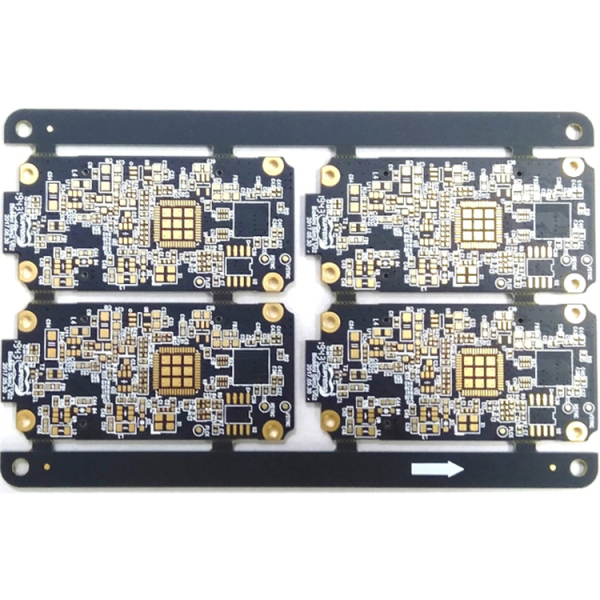
HDI is an abbreviation for high-density interconnection. It is a (technology) for the production of printed circuit boards. It is a circuit board with a relatively high line distribution density using BVH PCB technology. HDI is a compact product designed for small-capacity users. The Quick Turn PCB adopts a modular design that can be connected in parallel. One module has a capacity of 1000VA (1U height) and is naturally cooled. It can be directly placed in a 19" rack, and a maximum of 6 modules can be connected in parallel. The product adopts all-digital signal processing (DSP) technology and A number of patented technologies have a full range of load capacity and strong short-term overload capacity, regardless of load power factor and crest factor. Industrial Control Pcb,Custom Circuit Boards,Pcb Products,High Density Circuit Boards HAODA ELECTRONIC CO.,LIMITED , https://www.pcbhdi.com
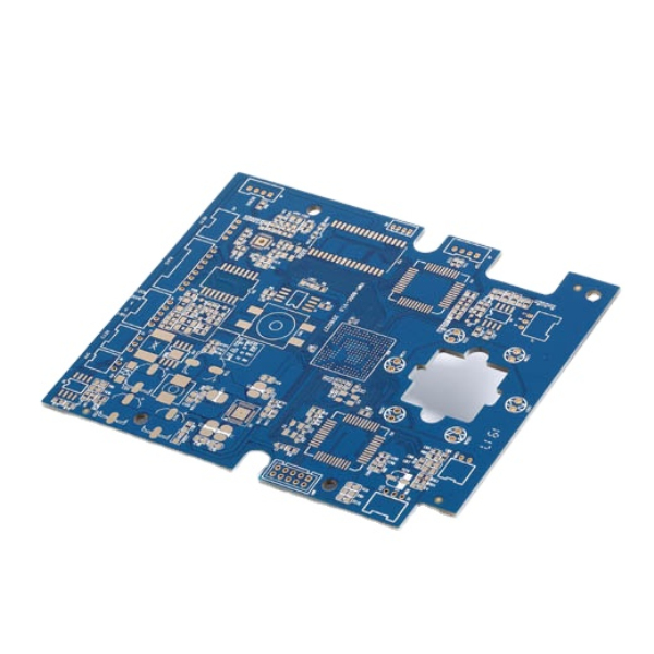
HDI PCB is a high-density interconnection (HDI) manufacturing printed circuit board. The printed circuit board is a structural element formed by insulating materials and conductor wiring. When the printed circuit board is made into the final product PCBA, the Originality Electronics IC, transistors (transistors, diodes), Electronic Resistor And Capacitor and various other electronic parts will be installed on it. With the help of wire connection, it is possible to form an electronic signal connection and function. Therefore, the printed circuit board is a platform that provides component connection and is used to accept the substrate of the connected parts.


Four Misunderstandings in FPGA Learning
1, not familiar with the internal structure of the FPGA, do not understand the basic principles of programmable logic devices.
Since the printed circuit board is not a general terminal product, the definition of the name is slightly confusing. For example, the motherboard for personal computers is called the motherboard and cannot be directly called the circuit board. Although there are circuit boards in the motherboard, it is not They are not the same, so when evaluating the industry, the two are related but cannot be said to be the same. Another example: because there are integrated circuit components mounted on the circuit board, the news media call it an integrated circuit board (IC board), but in essence it is not the same as a printed circuit board.
While electronic design is constantly improving the performance of the whole machine, it is also working hard to reduce its size. In small portable products ranging from mobile phones to smart weapons, "small" is the eternal pursuit. High-density integration (HDI) technology can make terminal product designs more compact, while meeting higher standards of electronic performance and efficiency. HDI is currently widely used in mobile phones, digital (camcorder) cameras, MP3, MP4, notebook computers, automotive electronics and other digital products, among which mobile phones are the most widely used.
HDI PCBs are generally manufactured using a build-up method. The more build-up times, the higher the technical level of the board. Ordinary HDI boards are basically one-time build-up. High-end HDI uses two or more build-up techniques, while using advanced PCB technologies such as stacking holes, electroplating and filling holes, and laser direct drilling. High-end HDI boards are mainly used in 3G mobile phones, advanced digital cameras, IC carrier boards, etc.