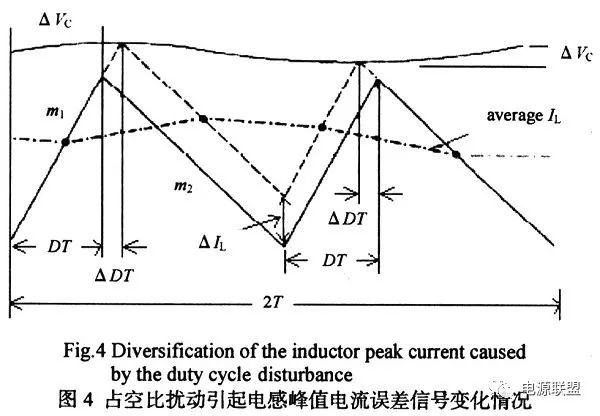
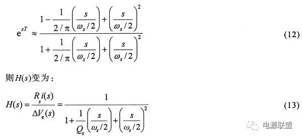
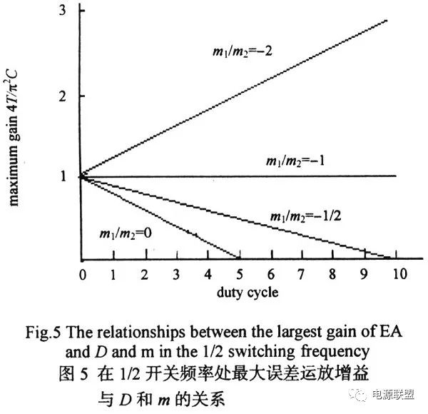
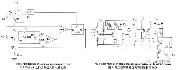
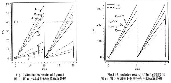
Due to its small size, light weight, high efficiency and stable performance, DC-DC switching power supply has been widely used in electronics, electrical equipment and home appliances, and has entered a period of rapid development. The DC-DC switching power supply uses a power semiconductor as a switch to adjust the output voltage by controlling the duty cycle of the switch. For the current inner loop control mode, Figure 2 shows the change of the inductor current when the system duty cycle is greater than 50% and the inductor current has a small step Δ厶, where the solid line is the inductor current waveform during normal operation of the system, and the dotted line The actual operating waveform for the inductor current. It can be seen that: 1) the inductor current error of the latter clock cycle is larger than the inductor current error of the previous cycle, that is, the inductor current error signal oscillates and diverge, and the system is unstable; 2) the oscillation period is twice the switching period, that is, the oscillation frequency It is 1/2 of the switching frequency, which is the origin of the subharmonic oscillation name. Figure 3 shows the variation of the inductor current when the system duty cycle is greater than 50% and the duty cycle has a small step AD. It can be seen that the system also exhibits subharmonic oscillations. When the system duty cycle is less than 50%, although the disturbance of the inductor current or duty cycle also causes the inductor current error signal to oscillate, this oscillation belongs to the damped oscillation. The system is stable. The reason for the subharmonic oscillation is qualitatively analyzed in the front, and it is now quantitatively analyzed. For Figure 1, Figure 4 shows the variation of the inductor peak current error signal caused by the duty cycle disturbance. Vc is the output signal of the error op amp. When the power transistor MO is turned on, the inductor current increases linearly, and Vc increases. On the contrary, when the power tube M0 is turned off, Vc decreases. It can be seen from Fig. 4 that when the duty ratio is asymmetrical under two consecutive clock pulses, the system will exhibit subharmonic oscillation. The relationship between ΔVc and ΔIL is derived. The duty cycle disturbance ΔD causes the change values ​​of the inductor current and the output voltage of the error op amp as shown in equations (1) and (2), respectively, from equations (1) and (2). It can be deduced that the relationship between Vc and ΔIL is as shown in equation (3): Where: T is the switching period; m1 is the peak current rising slope; m2 is the peak current falling slope absolute value; and seven is the sampling resistance. Since the subharmonic oscillation frequency is 1/2 of the switching frequency, the voltage loop gain at the 1/2 switching frequency will directly affect the stability of the circuit. Now derive the voltage loop gain of Figure 1. After the slope compensation is superimposed on the output of the error op amp, set the error voltage from ΔVc to ΔVe, so that the relationship between ΔVc and ΔVe can be derived, as shown in equation (4). . From equations (3) and (4), equation (5) can be obtained. In steady state, equation (6) can be derived, and equation (6) can be substituted into equation (5) to eliminate m1, and equation (7) is obtained. Where: m is the slope of the lower slope; 2 means that the subharmonic oscillation period is twice the switching frequency. It can be seen from Fig. 4 that ΔIL is a square wave with a period of 2T, and the amplitude of the first subharmonic should be multiplied by 4/π. Assuming a load capacitance of C, the small signal voltage gain from the error op amp output to the power supply output is If the error amplifier voltage gain is A, the voltage outer loop loop gain is According to the loop stability condition, the loop phase margin is zero at the l/2 switching frequency. If the loop gain is greater than 1, the system will have subharmonic oscillation, so the maximum gain of the error op amp is : It can be clearly seen from equation (8) that the maximum gain of the error op amp is a function of the duty cycle D and the slope compensation slope m. The relationship between the normalized error op amp maximum gain and D and m is shown in FIG. It can be seen that when m=O (no compensation), since the gain of the op amp cannot be less than 0, when the duty ratio is greater than or equal to 50%, the system will have subharmonic oscillation; when m=m2/2, D Subharmonic oscillation occurs at =100%, but oscillation occurs when D<100% in the actual circuit; when m=1 m2, the maximum gain of the error op amp is independent of the duty cycle. When the m is continuously increased, the stability of the loop is not affected, but the overcompensation affects the transient response characteristics of the system. The reasons and solutions for the subharmonic oscillations caused by the change waveform of the inductor current signal are studied above. It is now studied in more depth from the s-domain (or frequency domain) perspective. Set the sampling inductor current i to be converted into a voltage by the sampling resistor Rs, i(k) represents the current disturbance amount at the kth clock, and ΔVe(k+1) is the voltage control disturbance amount at the k+1th moment, which is sampled and held. Discrete time function: It can be seen from equation (10) that when there is no slope compensation, and m11, it means that one pole is outside the unit circle, and the current loop is unstable at this time. Convert H(z) to s domain transfer function: Where s represents the frequency. esT can use PadE to make a second-order approximation with Pade: In the formula, Qs=2/[π(2/α-1)], that is, the damping coefficient is 1/Qs=[π(m1-m2+2m)]/[2(m1+m2)]. Equation (13) is the current loop transfer function. Before the slope compensation, when m1(m2-m1)/2 is m>max[(m2-m1)/2]=m2/2, Qs is greater than 0. The pole of the loop transfer function will appear in the left half plane, and the system is not necessarily stable at this time. The system is stable only when the current loop has sufficient phase margin. When m2>m>m2/2, although the system is stable, the ringing current will still appear at this time. Only when m=m2, that is, the damping coefficient is π/2, the system can eliminate the ringing current in one cycle. Get a very good transient response. When m>m2, although the current loop phase margin increases, its bandwidth becomes smaller, that is, overcompensation occurs, which affects the response speed of the system. 2 Slope Compensation Method and Circuit Implementation In the past, the causes of subharmonic oscillations were studied from several aspects, and it was pointed out that the slope compensation can prevent the system from generating harmonic oscillations. The compensation method and its specific circuit implementation are now studied. Switching power supply slope compensation is divided into two modes: upper slope compensation and lower slope compensation. Figure 6 shows the principle of the lower slope compensation. The inductor peak current waveform with a duty cycle greater than 50% at the time of the lower slope compensation is given (the current small disturbance is the excitation signal). Compared to Figure 2, only Ve changes from a horizontal straight line to a lower slope. It can be seen from Fig. 6 that after the slope compensation is introduced, the amplitude of the current error signal is proportionally attenuated every one clock cycle, and finally disappears. Figure 7 shows the upper slope compensation principle, showing the inductor peak current waveform with a duty cycle greater than 50%. The compensation principle is to superimpose the slope compensation current b on the inductor peak current a to form the detection current c, so that the duty ratio is less than 50%, and the system is stabilized. Since the upper slope compensation circuit is relatively simple to implement, the upper slope compensation is generally employed. For slope compensation, the larger the slope, the faster the oscillation decays, but the compensation slope is too large, causing overcompensation. Over-compensation will increase the impact of slope compensation on the system switching current limit specification, thereby reducing the system's load capacity; on the other hand, over-compensation will affect the system transient response characteristics. Usually choose the slope compensation slope to be compromised as needed. For Buck and Flyback converters, the compensation ramp generally takes the peak current drop slope m2, Vout/L. Since the output voltage is constant, the compensation value is easy to calculate and constant. For the Boost circuit, the compensation slope also generally takes the peak current drop slope m2, ie (Vout-Vin)/L, but because the input voltage varies with the grid, the compensation value is required to follow the change of the input voltage. At this time, if the slope of the forced slope is fixed for the simple circuit design, over-compensation or under-compensation may occur, and the circuit may be reduced. Performance and resulting in waveform distortion. Because Buck and Flyback converter slope compensation principle circuit implementation is basically the same, so this paper only gives a kind of upper slope compensation Flyback slope compensation circuit (shown in Figure 8). FIG. 9 is a boost converter self-tuning slope compensation circuit proposed by the second author of the present invention. The simulation results of Figure 8 and Figure 9 are respectively carried out by Hspice simulation software. The simulation results are shown in Figure 10 and Figure 11, respectively. The oscillator frequency of Figure 10 is 100 kHz. M1 is the detection current curve, which slowly rises from 0 to 40 μA. The dashed lines a, b and c represent slope compensation signals with different slopes, and lines A, B and C are superimposed curves, respectively. It can be seen from Fig. 10 that by changing the ratio of the resistors R5 and R4, compensation signals having different slopes can be obtained. In Fig. 11, Vsense is the voltage generated by the peak current flowing through the sense resistor, and Vslope is the voltage generated by the sense current flowing through the sense resistor after the upper slope compensation. As can be seen from Figure 11, the different input voltages correspond to different compensation ramps, and the ramp change is proportional to the change in (Vout-Vin) to achieve the self-regulating function. 3 Conclusion
Wireless earphones are divided into three parts.The first part is the sound source,the second part is the receiver, the third part is the headset part,the function of this part is mainly used to convert the signal sent by the mobile phone or receiver into sound and then transmitted to the ears of people. Wireless earphones and wired earphones compared,the difference in sound quality is not big. Wireless is more convenient,mainly in the middle of the line is replaced by radio waves. Compared with wired earphones, wireless earphones have these advantages, abandon the trouble of wired,do the real wireless structure, freedom of movement.A variety of ways to use, a variety of functions, sound quality, noise reduction, call has been greatly improved.It is equipped with a portable case with both charging and storage functions. It is very convenient to charge the dead earphones automatically by putting them into the case.
Wireless Gaming Headphone,Wireless Gaming Earphones,Wireless Gaming Headset,Wireless Gaming Headset With Mic Henan Yijiao Trading Co., Ltd , https://www.yjusbhubs.com
Its control circuit topology is divided into current mode and voltage mode. Current mode control is widely used due to its fast dynamic response, simplified compensation circuit, large gain bandwidth, small output inductance and easy current sharing. Current mode control is divided into peak current control and average current control. The advantages of peak current are: 1) Transient closed-loop response is faster, and the transient response to input voltage change and output load change is faster; 2) Control loop Easy to design; 3) Simple and automatic magnetic balance function; 4) Instantaneous peak current limiting function. However, the peak inductor current may cause subharmonic oscillations in the system. Although many literatures have introduced this in some cases, there is no systematic study on subharmonic oscillations, especially the causes and specific circuit implementation. Subharmonic oscillations are systematically studied. The cause of the 1st harmonic oscillation is taken as an example of the PWM modulation peak current mode switching power supply (as shown in Figure 1, and the lower slope compensation structure is given). The causes of the subharmonic oscillation are analyzed in detail from different angles. 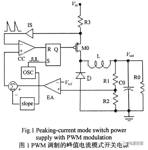






In this paper, the subharmonic oscillation of the peak current mode switching power supply is systematically studied from the qualitative and quantitative angles. When the duty ratio is greater than 50%, the current loop of the system oscillates at the 1/2 switching frequency, and the slope is introduced. After compensation, the transfer function of the current loop gain can ensure a good phase margin at 1/2 switching frequency to ensure system stability. Finally, the methods of avoiding subharmonic oscillations of upper slope compensation and lower slope compensation are analyzed. The specific slope compensation circuits and simulation results are given based on the three basic switching power supply topologies (Buck, Flyback and Boost).
The latest wireless headset has a professional learning scheme,can learn the functions of various home appliances remote control (TV, VCR, DVB, DVD, etc.),can also be used as a digital SET-top box remote control. Wirelessly listen to most electrical appliances with audio output. Using wireless earphones, you can enjoy exciting programs freely when the TV is silent.Place THE TRANSMITTER NEAR THE elderly, infants, patients and other people in need of care. Use the receiver to hear the voice of the person being cared for, and care is convenient and easy. Adopt THE ORIGINAL IMPORTED TRANSMITTING TUBE AND CORE technology, HIGH sensitivity ANTI-interference, strong signal, outstanding effect, effective range (less than) 30 meters, can be received by the wall.
