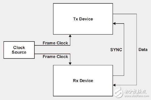
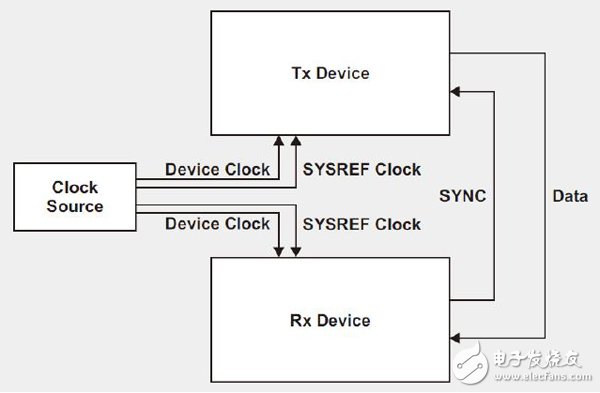
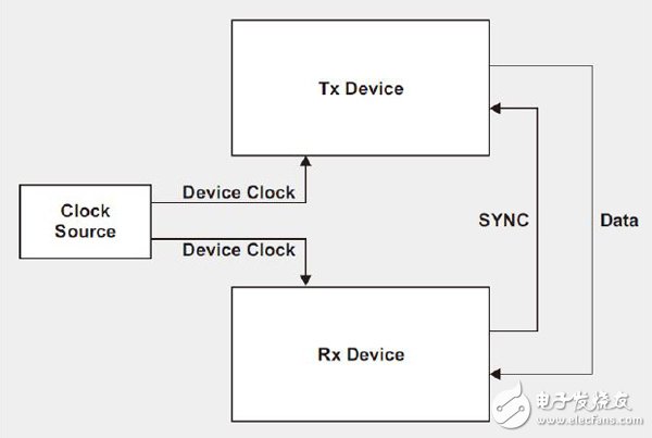
Those who use FPGAs in high-speed data capture designs have probably heard the name of the new JEDEC standard "JESD204B". Many engineers have recently contacted Texas Instruments to learn more about the JESD204B interface, including how it interacts with FPGAs and how JESD204B makes their designs easier to implement. This article describes the evolution of the JESD204B standard and how it affects system design engineers. High-speed data converter designers originally used a traditional single-ended CMOS interface and switched to a differential LVDS interface about a decade ago because of the higher data transfer rate (up to 200 Mbps for CMOS interfaces), which also improves signal line and power supply. Noise coupling. However, the disadvantage of the LVDS interface is that it consumes more power when the sampling speed is slower. Therefore, the CMOS interface has not been completely replaced, and it is still used today. Since the evolution of analog-to-digital converters must increase the sampling rate and channel density, the industry needs a faster and more energy-efficient digital interface than parallel LVDS, so the serial interface JESD204 was developed and passed JEDEC in April 2006. The JESD204 interface connects one or more data converters to a single digital logic device in a single-path, high-speed sequence with a transport rate of up to 3.125 Gbps, but must deliver common architecture frequencies to the converter and FPGA to ensure architectural synchronization. However, because JESD204 only supports one path and one sequence connection, the industry quickly found that the use was not as good as expected. Therefore, in April 2008, the standard was JESD204A, which can support multiple paths and multiple links, but the upper limit of the rate is still 3.125 Gbps. JESD204B was developed in July 2011 to overcome a number of system design challenges. In addition to significantly increasing the transmission rate to 12.5 Gbps, the new delay feature has been added to greatly simplify multi-channel synchronization. The JESD204B supports interface rates up to 12.5 Gbps, replacing the architectural frequency with the device frequency, and has three sub-collections. Sub-collection 0 is backward compatible with JESD204A, but the speed is limited, the delay function is not supported, and the SYNC signal also has a special frequency condition for error reporting (see Figure 1). Sub-set 1 initiates and combines the multi-architecture frequencies of the devices (as shown in Figure 2) by synchronizing the signal SYSREF to achieve data transfer synchronization and to ensure a known determined delay within the digital link. Figure 1 JESD204B sub-collection 0 interface Figure 2 JESD204B sub-collection 1 interface Subset 2 also uses the SYNC signal (Figure 3), but is limited by the frequency condition of the SYNC signal and is typically used when the data rate is below 500 MSPS. When the data rate exceeds 500 MSPS, Subset 1 is usually used and the SYSREF frequency is added. Figure 3 JESD204B sub-collection 2 interface The JESD204B-compliant receiver has an elastic buffer space that compensates for the skew of the sequencer/de-serializer channel, thus simplifying board configuration. The elastic buffer space stores data until the slowest channel data arrives, and then simultaneously releases data from each channel for digital processing. Because the data frequency is already embedded in the sequence data stream, time-delay management is available. JESD204B-compliant data converters stream data and transmit at a faster rate than legacy interfaces, so the number of pins required for data converters, processors, or FPGAs is significantly reduced, reducing package size and cost. The biggest advantage is that after reducing the number of pins, the channel on the circuit board is reduced, making the board configuration simpler and wiring easier. In addition, since the data frequency is embedded in the data stream and there is also an elastic buffer space in the receiver, the time lag management requirement is reduced, so that the configuration and wiring are further simplified, and it is no longer necessary to confirm whether the curves are equal in length. The JESD204B also extends the transmission distance because the distance between the logic device and the data converter can be extended after the delay condition is relaxed, avoiding any sensitive analog component impact. On the other hand, the JESD204B interface can be used with a variety of data converter resolutions, so there is no need to redesign the transceiver/receiver (Tx/Rx) board (logic device) whether it is an analog-to-digital converter or a digital-to-analog converter in the future. ). For low-transfer rate data converters, the CMOS interface consumes less power, and the JESD204B interface has several advantages over the traditional LVDS interface. So, is there an opportunity for survival in the LVDS interface? Simply put, the LVDS interface is still useful. Although the JESD204B standard simplifies multi-channel synchronization with a defined delay, some applications require as small a delay as possible (and even better without delay), and these applications (such as space applications such as radar) require immediate response or detection, so It is possible that the delay must be minimized. In this case, LVDS should be considered because JESD204B can be avoided to cause the data converter to delay during the data sequence. Stainless Steel Plate,304 Stainless Steel Plate,Stainless Steel Chequer Plate,Stainless Steel Decoration Plate ShenZhen Haofa Metal Precision Parts Technology Co., Ltd. , https://www.haofametal.com

