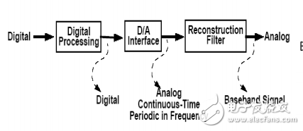
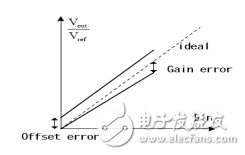
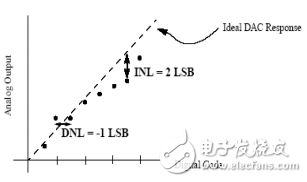
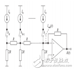
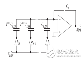
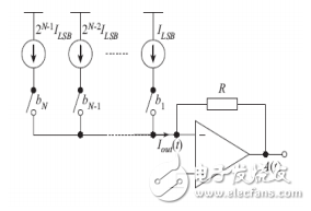
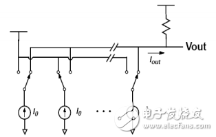
A digital-to-analog converter (DAC) converts a digital quantity into an analog quantity. The device that performs this conversion is called a digital-to-analog converter. This article will introduce the concept, principle, main technical indicators of the digital-to-analog converter and the characteristics of different types of DAC. 1 concept of digital to analog converter The digital quantity processed by the digital system is sometimes required to be converted into an analog quantity for practical use. This conversion is called "digital-to-analog conversion". The circuit that completes the digital-to-analog conversion is called a digital-to-analog converter, or DAC (Digital to Analog Converter). DAC working principle block diagram 2, the basic concept in DAC Resolution The resolution in the DAC is defined as the number of analog levels of all possible outputs at different input digital code values. The N-bit resolution means that the DAC can generate 2 N −1 different analog levels, in general it It refers to the number of digits of the input digital code. Offset and gain error The offset is defined as the value of the analog signal actually output when the 0 code value is input. The gain error is defined as the difference between the value of the ideal full-scale output and the value of the actual output when the offset is subtracted, as shown. DAC offset and gain error Precision The accuracy in the DAC is divided into absolute accuracy and relative accuracy. Absolute accuracy is defined as the difference between the ideal output and the actual output, including various offset and nonlinear errors. Relative accuracy is defined as the maximum integral nonlinearity error. Accuracy is expressed as the ratio of full scale, expressed in significant digits. For example, 8-bit precision means that the DAC error is less than 1/8 of the full scale of the DAC output. Note that the concept of precision is not related to resolution. A 12-bit resolution DAC may have a 10-bit accuracy; a 10-bit resolution DAC may have a 12-bit accuracy. Accuracy greater than resolution means that the transmission response of the DAC can be controlled more accurately. Integral Linearity (INL-Integral Nonlinearity) When the offset and gain errors are removed, the integral linearity error is defined as the deviation of the actual output transmission characteristic curve from the ideal transmission characteristic curve (a straight line). as the picture shows. DAC integral and differential linearity error Differential linearity error (DNL-DifferenTIal Nonlinearity) In an ideal DAC, each analog output change is a minimum of 1LSB, and the differential linearity error is defined as the deviation of 1LSB from each time the analog output changes minimally (except for gain errors and offsets). The DNL we define is for each digital input code value, and sometimes the largest DNL is used to define the DNL of the entire DAC. The ideal DAC has a differential linearity error of 0 for each digital input, and a minimum change output of 0.5 LSB to 1.5LSB for a DAC with a maximum DNL of 0.5LSB. As shown in the integral and differential linearity errors of the DAC. Glitch Impulse Area The maximum area under the jitter at the output after the input signal changes. Settling TIme Outputs the time required to experience a full-scale conversion within a specific tolerance of the final value. Monotonicity A monotonic DAC means that the DAC is always increased as the input digital code value increases the output analog level. If the maximum DNL is controlled within 0.5LSB, the monotonicity of the DAC is naturally guaranteed. Pseudo Dynamic Range (SFDR) SFDR is the Spurious Free Dynamic Range, the dynamic range of noise and harmonics. Both noise and harmonics are called spurious. 3 digital-to-analog conversion principle Each binary code input is converted into the corresponding analog quantity according to the weight of its weight, and then the analog quantity representing each bit is added, and the total analog quantity obtained is proportional to the digital quantity, thus realizing the digital quantity to Analog conversion. among them 4 The composition of digital-to-analog converters and the characteristics of different types of digital-to-analog converters The DAC consists primarily of digital registers, analog electronic switches, a bit-weight network, a summing operational amplifier, and a reference (or constant current source). Using the digital digits stored in the digital register, the analog electronic switches of the corresponding bits are respectively controlled, so that the digits of the digits of 1 generate a current value proportional to the bit weight on the bit weight network, and then the current values ​​of the operational amplifiers are used. Summing and converting to a voltage value. Depending on the weighting network, different types of DACs can be constructed, such as the weight resistor network DAC, the R–2R inverted T-resistor network DAC, and the single-value current-mode network DAC. The conversion accuracy of the weighted resistor network DAC depends on the reference voltage VREF and the accuracy of the analog electronic switches, operational amplifiers, and individual resistor values. Its disadvantage is that the resistance values ​​of the weight resistors are different. When the number of bits is large, the resistance values ​​are far apart, which brings great difficulty to ensure the accuracy, especially for the fabrication of integrated circuits, so the integrated DAC is This circuit is rarely used alone. 5 main technical indicators of analog to digital converter Conversion accuracy and conversion speed of the DAC: Conversion accuracy In the DAC, resolution and conversion error are generally used to describe the conversion accuracy. (1) Resolution Generally, the number of bits of the DAC is used to measure the resolution. Because the more bits, the more the output voltage vO is (2n), the more it reflects the subtle change of the output voltage. The higher. In addition, the resolution can be defined by the ratio of the minimum output voltage of 1 LSB that can be resolved by the DAC to the maximum output voltage, FSR. which is The smaller the value, the higher the resolution. (2) Conversion error The conversion error is the maximum deviation between the actual output analog voltage and the ideal value. This percentage of maximum deviation to FSR or a number of LSBs is commonly used. In fact, it is a comprehensive indicator of three kinds of errors. (3) Conversion speed The conversion speed is generally determined by the setup time. This is called settling time, which is the maximum response of the DAC, from the time when the input is abrupt all 0s to all 1s, and until the output voltage is stable within the FSR±1â„2 LSB range (or within the range indicated by FSR±x%FSR). Time, so use it to measure the speed of the conversion. 6 digital-to-analog converter composition The DAC consists primarily of digital registers, analog electronic switches, a bit-weight network, a summing operational amplifier, and a reference (or constant current source). Using the digital digits stored in the digital register, the analog electronic switches of the corresponding bits are respectively controlled, so that the digits of the digits of 1 generate a current value proportional to the bit weight on the bit weight network, and then the current values ​​of the operational amplifiers are used. Summing and converting to a voltage value. Depending on the weighting network, different types of DACs can be constructed, such as the weight resistor network DAC, the R–2R inverted T-resistor network DAC, and the single-value current-mode network DAC. 7 DAC's various topologies Resistance type: The structure is shown in Figure 1. Figure 1 shows an R-2R ladder network type converter. The advantage is that it achieves good linearity. Since all current sources are equivalent, we can use special additional techniques to make the error between them small, and the structure is much simpler than the resistor divider. The disadvantage is that the resistance is always non-linear and also contains the parasitic capacitance associated with the signal, making it difficult to achieve a perfect match. At the same time, the speed is limited by the output buffer, and the speed cannot be very high. Figure 1 Structure diagram of a resistive DAC Capacitor type: The structure is shown in Figure 2. The highest capacitance CN is 1 2N− times the lowest capacitance C1. The advantage is that the power consumption is small, and the matching accuracy is higher than the resistance. The main limiting factors are the capacitance mismatch, the on-resistance of the switch, the large RC delay, and the effect of the amplifier's limited bandwidth on the DAC speed. A major drawback of charge-distribution DACs is that the capacitance in the CMOS process is a large chip area. Finally, since the nature of the capacitance in the CMOS process is non-linear, the linearity of the total DAC will be suppressed. Suitable for medium and high precision. Figure 2 Structure diagram of a capacitive DAC Current type: The structure is shown in Figure 3. The advantage is that when the accuracy is less than 10 bits, the area can be made small, the speed is not limited by the amplifier bandwidth and the large RC delay, and the high speed can be achieved. Since all the current flows directly to the output, the energy is It is very efficient to use and easy to implement. Disadvantages are sensitivity to device mismatch and limited current source output impedance. Suitable for high speed broadband requirements. The output can also be converted to a voltage output without using an operational amplifier, as shown in Figure 4. This form allows the rate of the DAC to be unrestricted by the op amp bandwidth. Figure 3 Structure diagram of the current DAC Figure 4 output is directly converted by load resistor
LCD (short for Liquid Crystal Display) liquid crystal display. The LCD structure is to place a liquid crystal cell between two parallel glass substrates. The lower substrate glass is equipped with TFT (Thin Film Transistor), and the upper substrate glass is equipped with a color filter. The liquid crystal molecules are controlled by the signal and voltage changes on the TFT. Rotate the direction, so as to control whether the polarized light of each pixel point is emitted or not to achieve the purpose of display. LCD has replaced CRT as the mainstream, and the price has dropped a lot, and it has become fully popular.
According to data from CINNO Research, 2020 is expected to be the first year for mass production of mobile phones with fingerprint recognition under LCD screens.
LCD features:
(1) Low-voltage micro power consumption Lcd Tft,Tft Lcd Led Projector,Tft Lcd Library,LCD panels ESEN Optoelectronics Technology Co., Ltd, , https://www.esenlcd.com

 The decimal value that is converted to a binary number by bitwise expansion.
(2) The appearance is small and exquisite, the thickness is only 6.5~8mm
(3) Passive display type (no glare, no irritation to human eyes, and no eye fatigue)
(4) The amount of display information is large (because the pixels can be made small)
(5) Easy to colorize (reproduce very accurately on the chromatogram)
(6) No electromagnetic radiation (safe for the human body, conducive to information confidentiality)
(7) Long life (this kind of device has almost no deterioration problem, so the life is extremely long, but the life of the LCD backlight is limited, but the backlight part can be replaced)