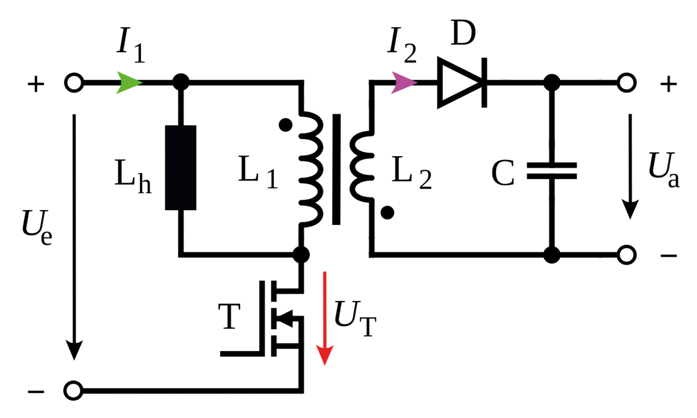
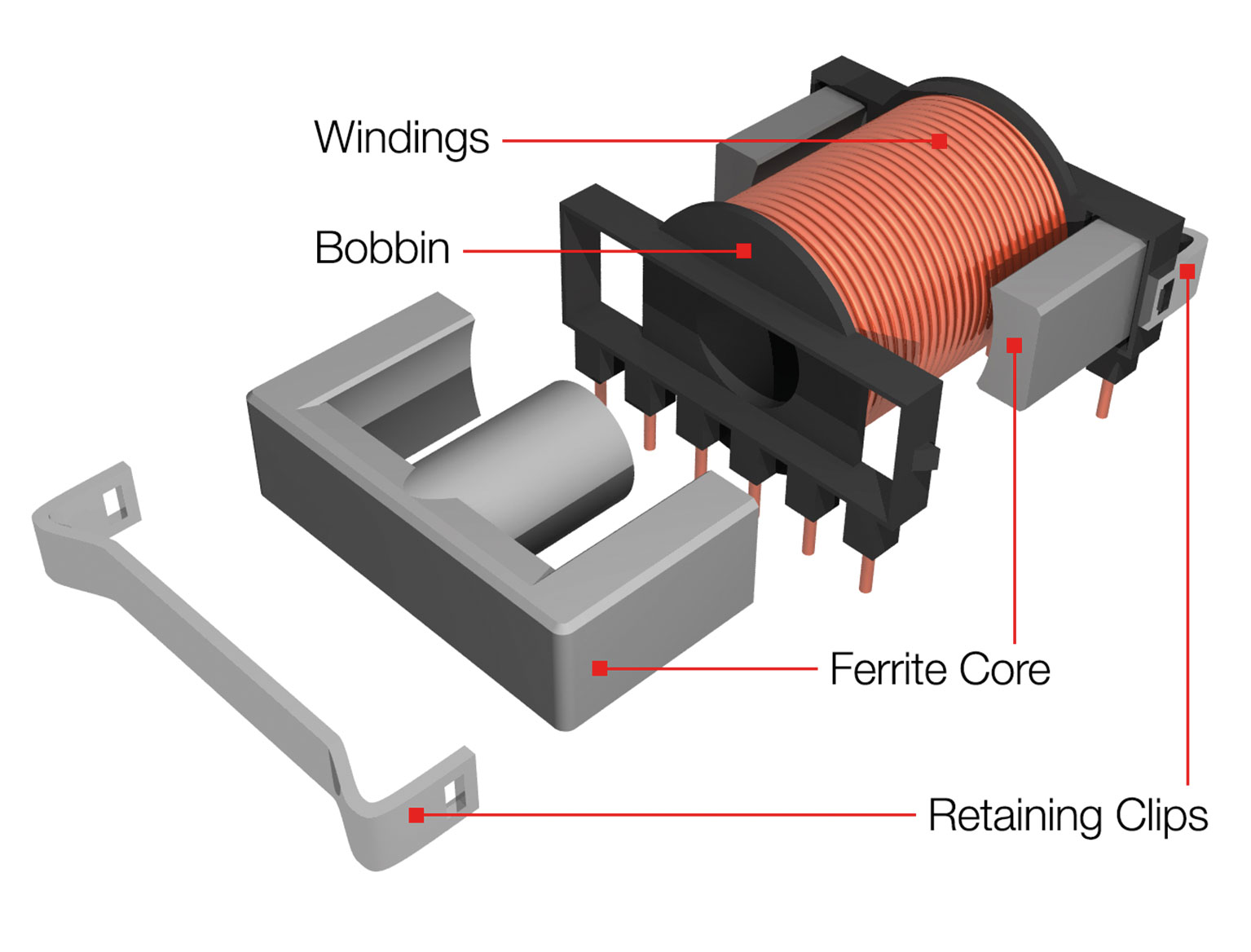
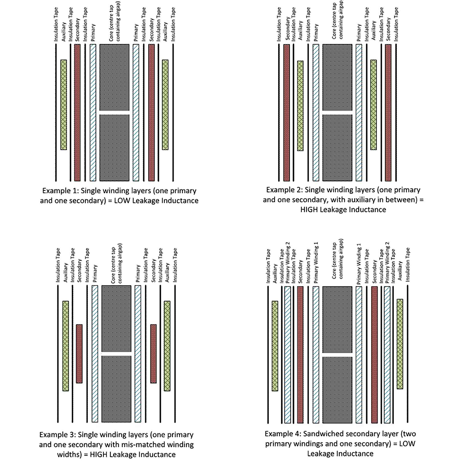
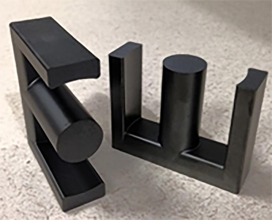
There are many possible topologies for switching power supplies (SMPS), but for circuits with loads below 150W, the most popular is the flyback converter. Some estimates even indicate that up to 75% of offline power supplies use a flyback topology. As a result, many power system designers face the challenge of developing flyback converter circuits. In order to achieve the best performance, meet electrical specifications, and stay within cost and space constraints, designers need to implement some form of customization in the design; the most important custom component of a flyback converter is a transformer. In the design engineering world, transformer design and prototype construction are often considered to be black art. For the layman, various parameters that affect transformer performance - from the choice of core material and dimensions to the placement of windings around the core - can be confusing. In fact, the transformer design process can be carried out in an orderly manner by applying a small number of important equations combined with a degree of trial and error, or "experience guessing." The design team at Future Electronics' EMEA System Design Center (SDC) in London, United Kingdom, has gained a lot of practical experience in developing customized power supplies for OEM customers. The purpose of this article is to share these experiences and illustrate how to optimize transformer design in a flyback converter circuit. Flyback topology: principle of operation Figure 1: Typical flyback converter circuit. (Source: Wald Dvorak, Wdwd, Wikimedia Commons, Creative Commons License Agreement) The flyback converter is an isolated buck-boost converter, as shown in Figure 1. it includes: A primary side switch, usually a MOSFET Two inductors in the form of primary and secondary windings wound on a magnetic core, such as Figure 2 shows. The windings rotate around a plastic frame that provides mechanical support and a set of pins for wire connections and through holes mounted on the PCB. In its operation, the correct arrangement of the two inductors is called "magnetically coupled inductor." However, due to the two independent windings, designers often refer to them as "flyback transformers." Strictly speaking, this is a misuse, but for the sake of convenience, this article will refer to it in this way. A secondary switch, usually a diode Output capacitance Figure 2: Inductor exploded view of the windings on two E-shaped cores. The air gap of the transformer is formed between the opposing faces of the core's center arm. (Source: Cyril Buttay, Creative Commons License Agreement) Feedback is usually achieved through optocouplers and compensation circuits for isolation barrier control. When the primary-side switch is turned on, the primary winding consumes current to generate a magnetic field that is easily transmitted to the small air gap at the center of the core through the low-reluctance core, where the stored magnetic energy accumulates. When the primary-side switch is opened, the stored magnetic energy induces a current that flows through the secondary winding and the output diode and flows to the load. The many advantages of this converter topology are the reasons for its widespread use: Isolated easily by flyback transformer and optocoupler feedback compensation Low component count and cost The turns ratio of the flyback transformer allows a high ratio between the input and output voltages, such as 3.3V output directly from the AC supply voltage input. A single power stage can provide multiple positive and negative polarity output voltage rails. The flyback topology supports boost and buck operations: it is a buck-boost topology. However, the flyback converter has some disadvantages. The most important ones are: The voltage stress on the MOSFET and the output diode is high, and there are large differences between the different designs. High peak currents and high voltage peaks of the two switching elements during switching transitions result in relatively high noise. The cross-coupling of the flyback transformer and the radiation from the windings may also generate noise. How Converter Specifications Affect Transformer Design The optimization of the flyback transformer is determined by the key parameters specified by the designer, namely: Output Power On-off level Peak and average current values ​​for primary and secondary windings (worst case considering minimum input voltage, maximum load) Primary side inductance Maximum flux density Number of turns However, before designers can begin designing a flyback transformer, they need to select the conduction mode: Continuous Conduction Mode (CCM), Discontinuous Conduction Mode (DCM), or Critical Conduction Mode (CRM). The transformer design process is the same for all three conduction modes, but in any power converter, the operation is different and in the case of flyback converters are basically different because of the transfer functions of the converters Not the same, it will affect feedback compensation. There is a large amount of literature that can guide the designer's choices, so this article does not explain conduction patterns in detail. The practical experience of Future Electronics SDC shows that the choice usually depends on: Size and cost pressures, in which case DCM has advantages due to its lower inductance requirements For low conduction losses and high efficiency requirements at higher output power levels, CCM is preferred in this case because peak and root-mean-square (RMS) output currents are low for any given output power value. The need to make further decisions early in the development process is the choice of core material. The main parameters affecting the choice of core material are the maximum flux density, reluctance, and cost. For a flyback transformer, the most commonly used magnetic material is ferrite. This is a cheap material with very low losses at switching frequencies up to 500 kHz. Ferrite cores become saturated at relatively low magnetic flux densities (typically around 0.4 T). This means that in designs using conventional ferrite cores, the flux density should remain no higher than 0.3T at the peak primary current in order to avoid saturation. The causes of loss and how to manage them In almost all power converter design projects, engineers are focused on minimizing power supply efficiency and power loss. In general, reducing losses helps reduce thermal stress and the need for cooling devices, improves system reliability, and enables the creation of smaller, lighter, and more economical end products. In a flyback converter, there are many sources of losses, including MOSFET and diode conduction, switching losses, output capacitor ripple current losses, snubber losses, and input and output filter losses. But in most cases, the largest part of the total loss is due to the flyback transformer. Therefore, efforts to reduce transformer losses will bring considerable benefits. First understand the various sources of loss within the flyback transformer, including: Copper loss: Caused by the DC and AC resistance of the copper wire used for the primary and secondary windings. Proximity loss: Due to the close-coupled current in a strong magnetic field, the current is concentrated in a portion of the cross-section of the copper wire. Leakage inductance: Magnetic leakage causes power loss. This must also be taken into account in circuit design because the magnitude of the leakage inductance directly affects the so-called "buffer loss." The basic requirement for avoiding magnetic field leakage is to position the air gap within the winding. Core material loss: caused by switching and inherent hysteresis of the core material. Copper loss The loss of winding copper wire is affected by the following factors: Current waveform, relative magnitude of DC and AC components The overall DC and AC resistance of the winding On-off level Proximity loss In particular, due to the so-called "skin effect", the high switching frequency and the relatively high AC component in the current waveform will increase the resistance. Skin effect causes high-frequency AC components to conduct on the outer surface of the guide wire, effectively reducing the cross-sectional area of ​​the conductor and thus increasing its resistance. Future evaluation by Future Electronics of an actual transformer design with a switching frequency of less than 100kHz shows that the use of single-strand copper wires with a diameter of ≤ 0.5mm can reduce the skin effect and copper loss. Proximity losses also increase the loss of copper wiring: In essence, conductors carrying high-frequency currents induce copper losses in adjacent conductors through the "proximity effect" phenomenon. This effect causes the copper loss to be compounded onto each additional layer in the multilayer winding. Therefore, in order to minimize the effect of proximity loss, the designer must keep the number of winding layers to a minimum: ideally, no more than two or three primary and secondary windings, especially when the current waveform has a high proportion of AC components This is the case with DCM operations. Leakage inductance is a function of the number of turns squared (N2) and the winding geometry. In order to minimize the leakage inductance of a given core and bobbin, designers should select a core with a suitable cross-sectional area to minimize the number of turns required to reach the target inductance. Another important step is to provide the best coupling between the primary winding and the secondary winding. The best results are obtained when the winding widths of the primary and secondary layers match and remain on adjacent layers, or when the secondary layer is sandwiched between two primary windings, as shown in FIG. Figure 3: Example of various winding configurations that produce low or high leakage inductance Core loss: Energy is required to change the magnetization of the core. Not all energy can be recovered in electricity. Part of the heat loss. This power loss can be seen as the hysteresis of the BH loop. Losses are usually proportional to changes in flux density (ΔB) and the square of the switching frequency (Fsw2). For a typical magnetic element, there is a tradeoff between saturation flux density and core loss. Using a material with a high operating flux density can reduce size, weight, and cost. For example, silicon steel cores typically have a saturation flux density of 1.5-2T. Unfortunately, such core materials also have high core losses. In contrast, the ferrite core is a ceramic material with a saturation magnetic flux density in the range of 0.25-0.5T. However, due to its higher resistivity, its core loss is lower. Commonly used ferrite core materials for flyback transformers include Ferrokecube's 3C90 and Magnetics® R materials, as shown in Figure 4. Figure 4: 70mm x 54mm Magnetics® Ferrite E Core Material data sheets provide curves showing core losses at various switching frequencies, typically plotted as core losses (in kW/m3) in ΔB (in Tesla), which can be used to estimate any given The core loss in the application. All the loss factors considered above also have an effect on the calculation of the core size. Off-the-shelf technical documents explain various methods for determining the size of the magnetic core. In the experience of Future Electronics, if the space and cost allow, it is better to start with a slightly larger core size, because it can reduce the number of turns, core loss and leakage inductance. In addition, it is best to choose a skeleton that provides the best winding length-height ratio: this minimizes the number of winding layers required. Next step: Hands-on build prototype This article outlines important theoretical considerations and design decisions that must be considered when designing a flyback transformer on paper. At the same time, it also provides some guidance on the practical experience of Fu-Chang electronic transformer design and related influencing factors (such as core size and winding arrangement). What is the Patch Panel? Why is the good
choice for your Server Center and Data Center?
A patch panel is a steel panel with a
number of ports helps organize a group of cables. Each of those ports includes
a wire that goes to a different location. Patch panel could be small size with
2 ports, or very large size with hundreds of ports. They could also be
installation for fiber optic cables, RJ45 cables, CAT5E / CAT6 / CAT6A/ CAT7 /
CAT8 Ethernet cables, and many others.
CAT6 Patch Panel,patch panel cat6,10 Inch 1U Patch Panel,Home Network Patch Panel NINGBO UONICORE ELECTRONICS CO., LTD , https://www.uonicore.com


