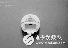
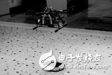
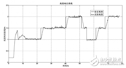
Circuit protection techniques and board layout strategies help improve security, reliability, and connectivity. Wearable technology has a weakness that is unlikely to occur in the Internet of Things: the body generates static electricity while moving. Static electricity can damage sensitive electronic devices that support IoT applications. To understand this problem, we started with the Human Body Discharge Model (HBM) and used to describe the sensitivity of integrated circuits to electrostatic discharge (ESD) damage. The most common HBM concept used is the experimental model defined in the military standard MIL-ST D-8 8 3 , Method 3015.8, Electrostatic Discharge Sensitivity Classification. A similar international HBM standard is JEDEC JS-001. Both the JEDEC JS-001 and the MIL-STD-883 simulate a charged human body with a 100pF capacitor and a 1.5kΩ discharge resistor. During the test, the capacitor was fully charged from 250 V to 8 kV and then discharged through a 1.5kΩ resistor in series with the device under test. Since wearable devices are designed to be used snugly, they continue to suffer from electrostatic shocks caused by close interaction with the user. Without proper protection, the sensor circuit, battery charging interface, button or data input/output port of the wearable device may be damaged by electrostatic discharge (ESD) similar to that produced in the HBM test. Once the wearable device fails, the functionality and reliability of the entire network is also affected. Advanced circuit protection technology and board layout strategies protect wearables and their users. Applying these recommendations early in the design process will help circuit designers improve the performance, security, and reliability of their wearable technology designs and help build a more reliable IoT. One design challenge for wearable device circuit protection is that wearable devices are becoming smaller and smaller. In the past, large structure diodes and large package sizes were required (eg Figure 1 TVS diode two structures Figure 2 IEC 61000-4-2 rating Designers should choose unidirectional diode configurations whenever possible because they perform better in negative voltage ESD strike events. During a negative voltage ESD strike, the clamp voltage will be based on the forward bias of the diode (typically less than 1.0 V). Conversely, the bidirectional diode configuration provides a clamp voltage that is based on the reverse breakdown voltage during a negative voltage surge and is higher than the forward bias of the unidirectional diode. Therefore, the unidirectional configuration can greatly reduce the pressure on the system during a negative voltage surge. Reasonably determine the diode position. Most wearable designs do not require the use of board-level T VS diodes on each integrated circuit pin. Instead, the designer should determine which pins are exposed to possible ESD events that may occur to the user. If the user can access the communication/control line, this can be a way for ESD to enter the integrated circuit. Typical circuits that tend to exist in this way include USB, button/switch control, and other data buses. Since the addition of these discrete device devices requires board space, devices that can be packaged in the 0201 or 01005 package are required. For some wearable applications, a space-saving multi-channel array can be used. Regardless of the package type used, the ESD suppressor should be positioned as close as possible to the ESD source. For example, the protection of the USB port should be close to the USB connector. Shorten the trace length. Trace routing is very important in the design of TVS diode protection for integrated circuit pins. Unlike lightning transients, ESD does not release large amounts of current for long periods of time. When handling ESD, be sure to transfer charge from the protected circuit to the ESD reference point as soon as possible. The primary factor is the length of the trace from the signal line to the ESD device and from the ESD device to ground, rather than the trace width of the ground. To limit parasitic inductance, the trace length should be as short as possible. Parasitic inductance can cause induced overvoltage, which is a short voltage spike that can reach hundreds of volts if the stub is long enough. Recent advances in packaging technology include the ability to mount directly in the data lane? The DFN contour so that the pile line is no longer needed. Understand the definition of the Human Body Discharge Model (HBM), the Machine Discharge Model (MM), and the Charged Device Model (CDM). In addition to the HBM model, MM and CDM are also experimental models that describe the ESD tolerance of integrated circuits running portable or wearable devices. Many semiconductor manufacturers believe that the MM model is outdated. People tend to track HBM in terms of robustness and resulting failure modes, although some manufacturers still use it. CDM is another alternative model for HBM. Unlike the interaction between the analog and the integrated circuit, the CDM analog integrated circuit slides toward the direction or tube and then touches the grounded surface. Devices classified by CDM contact the charge at a specified voltage level and then test for survival. If the device is still functioning properly, continue testing it at the next voltage level until it fails. CDM was standardized by JEDEC in JESD22-C101E. Chips, including processors, memory, and ASICs, are described in one or more of these three models. Semiconductor suppliers use these models during manufacturing to ensure the robustness of the circuit. For suppliers, the current trend is to reduce the level of voltage testing because it saves wafer space and because most vendors adhere to strict internal ESD policies. Strict ESD policies can benefit suppliers by running lower on-chip ESD protection, and circuit designers are still sensitive to application-level ESD, and never fail due to on-site ESD or user-induced ESD. To protect highly sensitive integrated circuits, designers choose protection devices that not only prevent enhanced electrostatic stress, but also provide a sufficiently low clamping voltage. The following parameters should be considered when evaluating an ESD protection device: 1. Dynamic Resistance: This parameter describes the ability of diode clamping to transfer ESD transients to ground. It can help determine how low the resistance will be after the diode is turned on. The lower the dynamic resistance, the better. 2. IEC 61000-4-2 rating: The TVS diode supplier determines the value of this parameter by increasing the ESD voltage until the diode fails. The point of failure describes the robustness of the diode. The higher the value of this parameter, the better. More and more Littelfuse TVS diodes can reach contact discharge voltages of 20 kV or even 30 kV, far exceeding the highest levels specified by IEC 61000-4-2 (level 4 level contact discharge voltage is 8 kV, see Figure 2). As the wearable market continues to grow and new devices continue to evolve, so does the need for circuit protection. In fact, considering ESD protection and proper board layout early in the design process is more important than ever. Small circuit protection devices such as TVS diodes will effectively protect sensitive integrated circuits inside wearable devices and maintain the value of the IoT ecosystem. Reliable long-term tracking algorithm. The starting point of the algorithm research is that the existing tracking algorithm or detection algorithm can not track the target for a long time. Kalal creatively combines tracking algorithms and detection algorithms to solve the problems of deformation, partial occlusion, etc. of the tracking target during the tracking process. At the same time, the "significant feature points" of the tracking module are continuously updated through an improved online learning mechanism. Target model and phase of the detection module The aircraft recognizes the ground robot The aircraft remains on the ground robot Throttle stroke and aircraft height Aircraft height control response curve based on switch control In this system, in order to maintain a good tracking effect. Based on the position of the ground robot in the image, a PD controller is introduced to keep the aircraft above the ground robot. The input of the controller is the pixel position in the center of the camera screen. The feedback value is the position of the ground robot actually captured in the image. The control block diagram is shown in Figure 7. The ground robot is kept in the center of the image according to the experimental adjustment of the PD parameters. Figure 8 shows the ground robot identified by the aircraft, and Figure 9 shows that the aircraft is tracking the ground robot. According to the actual aircraft experiment and the description of the Wukong control system, the test to the throttle signal has a corresponding relationship with the actual lifting of the aircraft, as shown in Figure 10. The duty cycle of the throttle PWM signal varies from 1000 to 2000. When it is between 1450 and 1550, the Wukong control system will automatically lock the current height of the aircraft. According to this feature, the switch controller is designed when the height is lower than The set value sets the duty cycle molecule to 1580, so the aircraft will slowly rise. When the height is higher than the given value, it is set to 1430, so that the aircraft slowly descends. And set the actual value to 5cm above and below the given value without control, that is, automatically lock the current height. As shown in Fig. 11, when the test value is switched from 0.5m to 1m to 1.5m, the aircraft can reach the given value in time. When the rudder is being steered, the height of the aircraft will change and the controller can be adjusted to reach the set height in time. In Figure 11, the straight line indicates the given height, the green line indicates the actual height of the aircraft, and the height controller is turned on near time 10s. Based on the 7th generation of the International Air Robot Competition, this paper proposes an implementation method of airborne equipment, and introduces the hardware platform and software module of the method in detail. This method completes positioning, height control, obstacle avoidance, and single ground robot identification and tracking. The aircraft has limited endurance and certain requirements for the competition time. Therefore, to complete the catch-up target of the a-stage of the competition, the upper-level strategy module needs further improvement. The b-stage of the game increases the same game of the aircraft, so more experiments are needed to increase the robustness of the system. Bushing Cover For Electrical Connections
Product functions:
Avoid electric shock caused by exposed electrical contacts.
Prevent short circuit caused by foreign bodies such as branches or small animals crawling.
Eliminate acid rain corrosion of transformer contacts (in recent years, the incidence of acid rain in China has increased significantly, and even the acidity PH is no more than 3, equivalent to acetic acid), eliminate the operation failure caused by this.
Dustproof, anti-theft electric function.
Applications:
Provide
insulation and protection for electrical connections.
Supply
protection and insulation in switchgear and substations.
Features:
1.Suitable for 1-35KV.
We are the professional manufacturer of Electrical Tapes,Insulating Tape and Special Adhesive in China for more than 25 years,if you want to know more information about our company and products, please visit our website.
Bushing Cover For Electrical Connections,High Voltage Bushing Covers,Insulating Bushing Electrical,Bushing Connector CAS Applied Chemistry Materials Co.,Ltd. , https://www.casac1997.com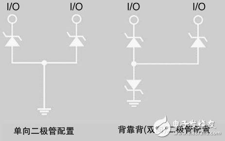

2.Radiation cross linking materials (Polyolefin or EPDM rubber ).
3.Quick and easy installation.
4.Avoid short circuit and leakage.
5.Facilitate routine inspection and maintenance.
6.Resistant to moisture and dust.
7.Meet RoHS Stand.
8.Customized.